Laser processing method and chip

a technology of laser processing and chip, applied in the field of laser processing, can solve the problems of inability to accurately cut objects, etc., and achieve the effects of preventing fractures, shortening the approach distance, and shortening the tim

Active Publication Date: 2008-01-03
HAMAMATSU PHOTONICS KK
View PDF13 Cites 81 Cited by
  • Summary
  • Abstract
  • Description
  • Claims
  • Application Information

AI Technical Summary

Benefits of technology

[0015]In the laser processing method in accordance with the present invention, the third modified region may be formed along substantially the whole line to cut or one end part thereof. Since a tensile stress is generated toward both sides of the line to cut in the part between the first and second modified regions in the object as mentioned above, a fracture may advance over substantially the whole part between the first and second modified regions if only a small part of the third modified region positioned between the first and second modified regions is formed. Therefore, forming the third modified region along substantially the whole line to cut can prevent fractures from being stopped advancing by some causes and reliably form fractures over substantially the whole part between the first and second modified regions. Forming the third modified region along one end part of the line to cut, on the other hand, can form fractures over substantially the whole part between the first and second modified regions while further shortening the time required for forming the modified regions in the object.
[0016]Preferably, in the laser processing method in accordance with the present invention, the third modified region is formed such as to be biased toward one of the first and second modified regions closer to the laser entrance surface where the laser light is incident in the object. If the third modified region positioned between the first and second modified regions is formed, fractures initially advance from the third modified region to one of the first and second modified regions closer to the third modified region and then from the other modified region, which is farther from the laser light entrance surface, to the one modified region closer to the laser light entrance surface. (In the following, the distance required until a fracture advances from the other modified region to the one modified region along the line to cut will be referred to as “approach distance”.) When the third modified region is formed such as to be biased toward one of the first and second modified regions closer to the laser light entrance surface, fractures can advance with a relatively short approach distance from the other modified region, which is farther from the laser light entrance surface, to the one modified region closer to the laser light entrance surface. Such a shorter approach distance enables a relatively small external force to cut the object along the line to cut.

Problems solved by technology

However, laser processing methods such as one mentioned above may fail to accurately cut the object depending on the thickness, cleavage characteristic, and the like of the object, for example.

Method used


Image

  • Laser processing method and chip
  • Laser processing method and chip
  • Laser processing method and chip

Examples


first embodiment

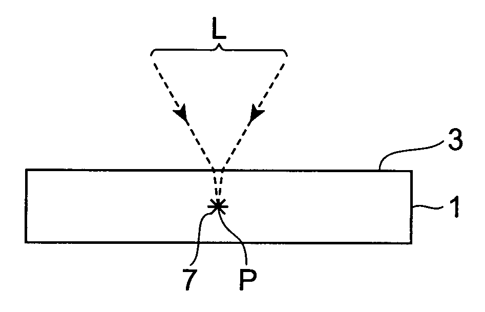
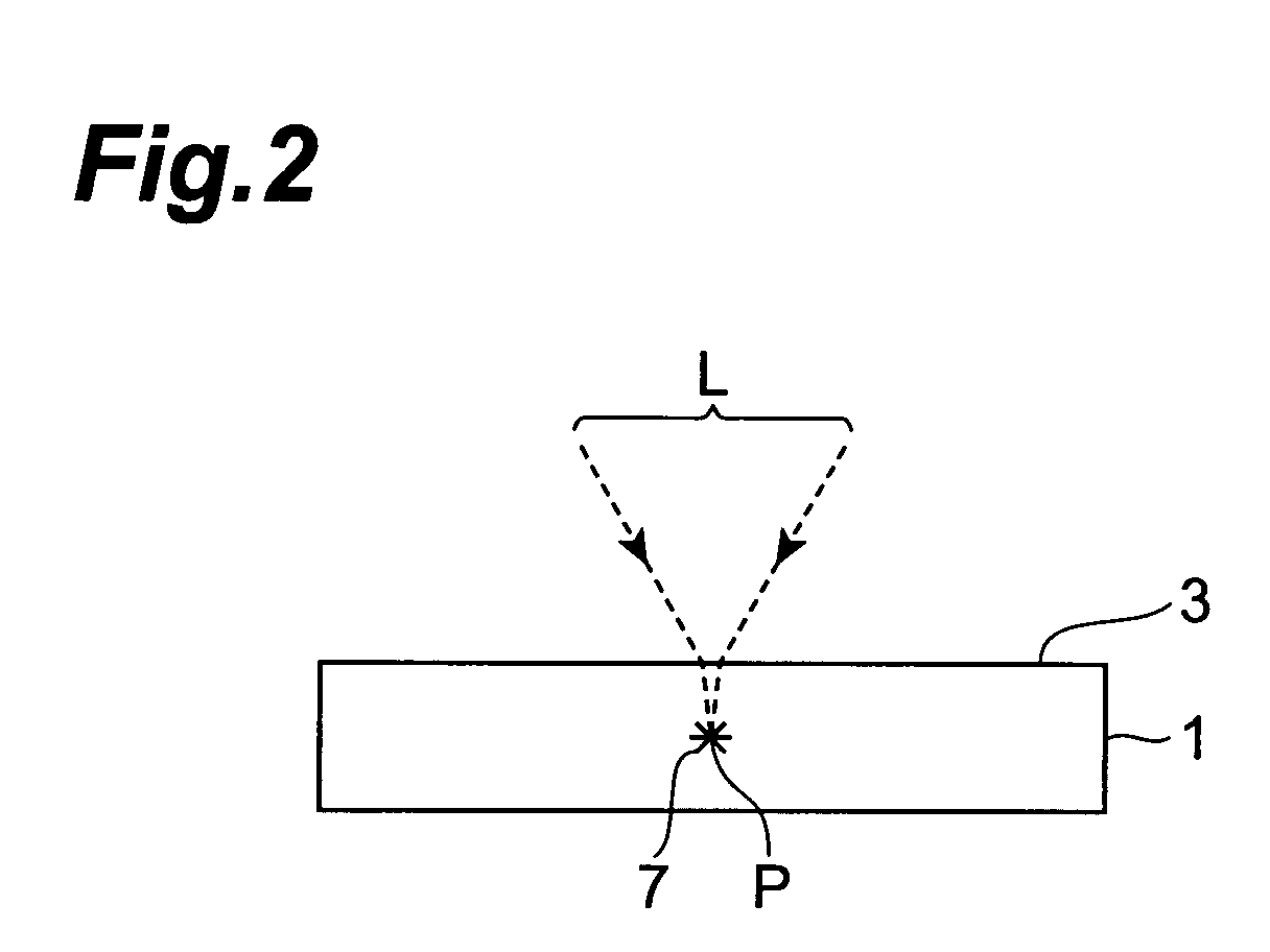
[0105]As shown in FIGS. 14 and 15, an object to be processed 1 comprises a silicon wafer 1, and a functional device layer 16 which is formed on the front face 11a of the silicon wafer 11a while including a plurality of functional devices 15. The silicon wafer 11 has such a crystal orientation that fractures are easy to extend in a direction different from its thickness direction t. Specifically, the silicon wafer 11 is a crystal structure having a cleavage plane in a direction parallel to its thickness direction and tilted with respect to a plane including a line to cut 5 which will be explained later, while fractures are likely to extend in a direction along the cleavage plane. Here, the front face 11a of the silicon wafer 11 is a (111) surface.

[0106]A number of functional devices 15, examples of which include semiconductor operating layers formed by crystal growth, light-receiving devices such as photodiodes, light-emitting devices such as laser diodes, and circuit devices formed ...

second embodiment

[0119]The laser processing method in accordance with a second embodiment of the present invention will now be explained. The laser processing method in accordance with the second embodiment differs from the laser processing method in accordance with the first embodiment shown in FIGS. 16 and 17 in that the modified region M4 is not formed. Specifically, the laser processing method in accordance with the second embodiment forms a modified region at a position deeper from the laser light entrance surface within the object along lines to cut, a modified region at a position shallower from the laser light entrance surface, and a modified region between these modified regions, and then cuts the object. This also has an effect similar to that mentioned above of preventing the end part of the cut section on the laser light entrance surface side from deviating greatly from the lines to cut when cutting the object as shown in FIG. 19(a).

third embodiment

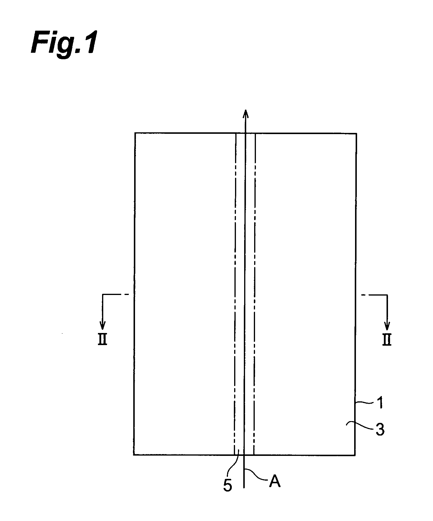
[0120]The laser processing method in accordance with a third embodiment of the present invention will now be explained. The laser processing method in accordance with the third embodiment differs from the laser processing method in accordance with the first embodiment shown in FIGS. 16 and 17 in that a plurality of modified regions are sequentially formed from the opposite side of the laser light entrance surface to the laser light entrance surface side before forming the modified region M1. Specifically, for example, the laser processing method in accordance with the third embodiment uses an object to be processed having a thickness of 250 μm, sequentially forms 11 rows of modified regions from the position of 67 μm to the position of 23 μm, the 12th row of modified region at the position of 7 μm, the 13th row of modified region at the position of 13.5 μm, and the 14th row of modified region at the position of 10 μm while taking the laser light entrance surface as the origin (the p...


PUM

PropertyMeasurementUnit
outer diameteraaaaaaaaaa
thicknessaaaaaaaaaa
sizeaaaaaaaaaa

Abstract

An object to be processed can be cut highly accurately along a line to cut.
An object to be processed 1 is irradiated with laser light while locating a converging point within a silicon wafer 11, and the converging point is relatively moved along a line to cut 5, so as to form modified regions M1, M2 positioned within the object 1 along the line to cut 5, and then a modified region M3 positioned between the modified regions M1, M2 within the object 1.

Description

BACKGROUND OF THE INVENTION[0001]1. Field of the Invention[0002]The present invention relates to a laser processing method for cutting a planar object to be processed along a line to cut, and a chip.[0003]2. Related Background Art[0004]Known as a conventional laser processing method is one irradiating a planar object to be processed with laser light while locating a converging point within the object, thereby forming a plurality of rows of modified regions to become a cutting start point within the object along a line to cut in the object (see, for example, Japanese Patent Application Laid-Open No. 2004-343008).SUMMARY OF THE INVENTION[0005]However, laser processing methods such as one mentioned above may fail to accurately cut the object depending on the thickness, cleavage characteristic, and the like of the object, for example.[0006]It is therefore an object of the present invention to provide a laser processing method which can highly accurately cut an object to be processed alo...

Claims


Application Information

Patent Timeline
Patent Type & Authority Applications(United States)
IPC IPC(8): B23K26/16B28D5/00B23K26/38C03B33/09
CPCB23K26/4075C03B33/0222B23K2201/40B23K26/0057B23K26/063H01L21/78B23K26/0622B23K26/40B23K26/53B23K2101/40B23K2103/50B23K26/361H01L21/67092H01L21/76
Inventor SUGIURA, RYUJISAKAMOTO, TAKESHI
Owner HAMAMATSU PHOTONICS KK
Why Eureka
Try Eureka