Liquid crystal display device

a liquid crystal display and display device technology, applied in non-linear optics, instruments, optics, etc., can solve the problems of reducing the size of the display device, consuming low power, and reducing the efficiency of the visual inspection of the sealant, so as to prevent the generation of defects in the sealant and allow effective visual inspection. , the effect of preventing the generation of defects

Active Publication Date: 2008-01-03
LG DISPLAY CO LTD
View PDF13 Cites 29 Cited by
  • Summary
  • Abstract
  • Description
  • Claims
  • Application Information

AI Technical Summary

Benefits of technology

[0016]An object of the embodiments of the invention is to provide a liquid crystal display device that allows effective visual inspections of a sealant and prevents defect generations in a sealant.

Problems solved by technology

Cathode Ray Tubes (CRTs), which are traditionally utilized as information display devices, have advantages in functions and cost, but have disadvantages in size miniaturization and portability.
In particular, LCD devices advantageously become smaller and lighter and consume low power, and accordingly receive attentions as replacement for overcoming the disadvantages of the CRTs.
However, the LCD device having such a structure may encounter the following problems.
As a result, a visual inspection cannot be performed effectively on the sealant after the completion of the LCD production process due to the common voltage line formed of an opaque metal and the overlap between the common voltage line and the sealant.

Method used


Image

  • Liquid crystal display device
  • Liquid crystal display device
  • Liquid crystal display device

Examples


first embodiment

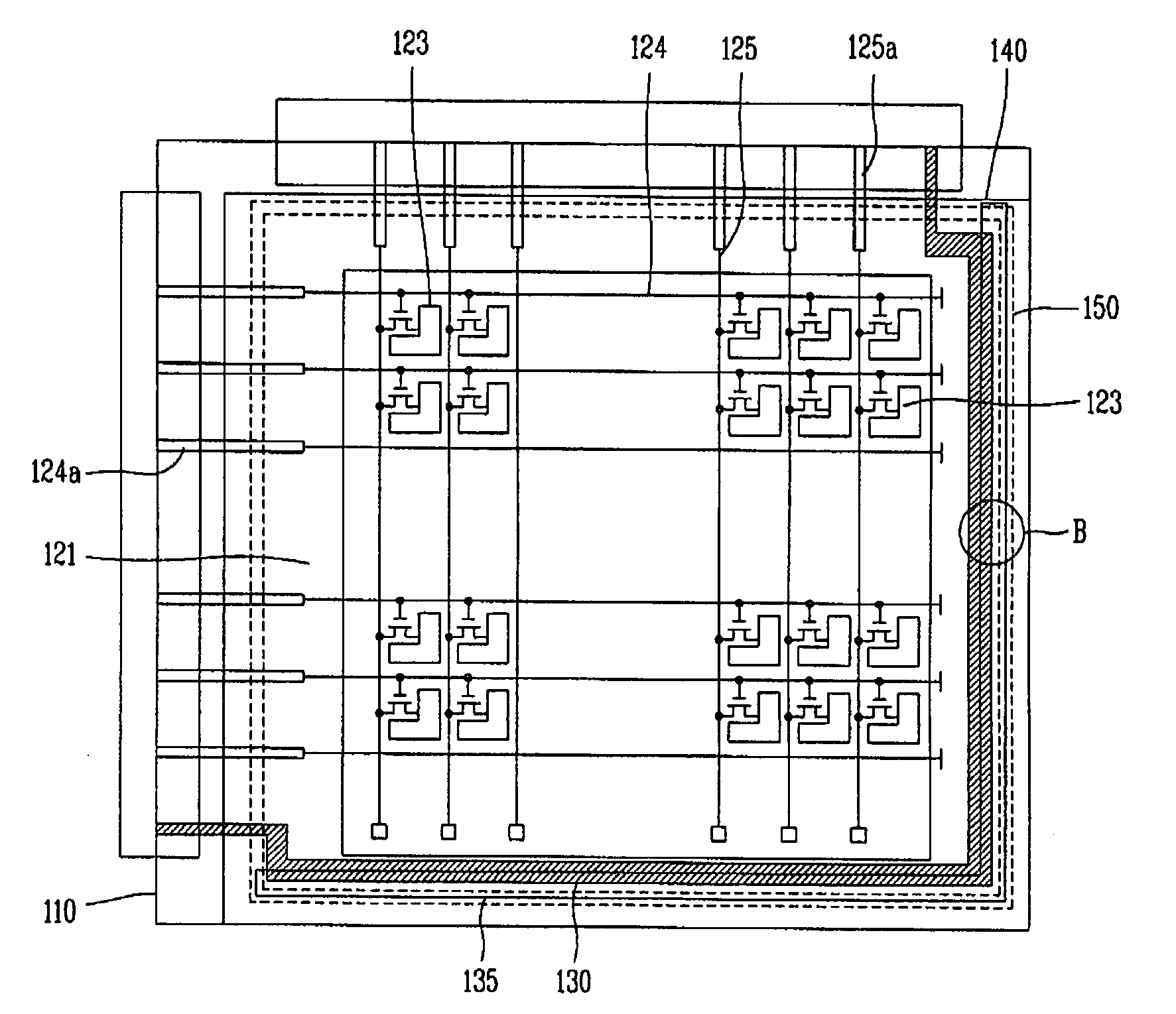
[0038]FIGS. 4A and 4B are plane view schematic diagram illustrating an LCD device in accordance with the invention. In FIG. 4A, an LCD device includes a lower substrate 110, an upper substrate 140 and a liquid crystal layer (not shown) interposed between the lower and upper substrates 110 and 140. The lower substrate 110 is bonded onto the upper substrate 140 by a sealant 150. The sealant 150 may be printed or coated by a screen printing method or a dispensing method on one or both of the lower substrate 110 or the upper substrate 140.

[0039]The lower substrate 110 includes a plurality of gate lines 124 and data lines 125 arranged thereon and defining a plurality of pixel regions. The lower substrate 110 also includes pixel electrodes 123 arranged therein the pixel regions and a thin film transistor (TFT) arranged in each of the pixel regions. Accordingly, by applying a signal to the TFT from the exterior via the gate lines 124, the TFT is controlled to selectively apply an image sig...

third embodiment

[0072]FIG. 9 is a plan view showing the LCD device according to this invention and FIG. 10 is an partially enlarged plan view of C-region of FIG. 9. In this embodiment, the common voltage line is made of the opaque metal and directly contacted with the sealant. In order to observe the shape of the sealant, in this invention, the window for observing the sealant is formed in the opaque common voltage line. This structure is described in detail as follow.

[0073]As shown in FIG. 9, the common voltage line 330 is formed along two sides, three sides, or all sides of the lower substrate 310, and the sealant 350 is formed in the outside of the lower and upper substrates 310 and 340 to attach thereof. The common voltage line 330 is made of opaque metal and the sealant 350 is overlapped with a part of the common voltage line 330.

[0074]As shown in FIG. 10, the common voltage line 330 includes a plurality of protrusions 330b protruded from a main common voltage line portion 330a. The sealant 35...


PUM

PropertyMeasurementUnit
transparentaaaaaaaaaa
insulatingaaaaaaaaaa
conductiveaaaaaaaaaa

Abstract

A liquid crystal display module includes an observation region to allow a visual inspection be performed after bonding of the substrates for inspecting the sealant that may be otherwise blocked by the common voltage line. An embodiment of a liquid crystal display device includes a first electrode on a first substrate, a second electrode and a third electrode on a second substrate, the second electrode electrically contacting the first electrode at a first portion and the third electrode at a second portion, and including a transparent conductive material, a sealant attaching the first and second substrates together in a sealant region, the sealant between the first and second electrodes and the sealant including a plurality of conductive balls for electrically connecting the first and second electrodes, and a liquid crystal layer between the attached first and second substrates and within the sealant.

Description

[0001]The invention claims the benefit of Korean Patent Application Nos. 10-2006-0061597 and 10-2007-055705 filed in Korea on Jun. 30, 2006 and Jun. 7, 3007, which are hereby incorporated by reference in their entirety.BACKGROUND OF THE INVENTION[0002]1. Field of the Invention[0003]Embodiments of the invention relate to a liquid crystal display device, and more particularly, to a liquid crystal display device that allows effective visual inspections of a sealant and prevents defect generations in a sealant.[0004]2. Discussion of the Related Art[0005]Cathode Ray Tubes (CRTs), which are traditionally utilized as information display devices, have advantages in functions and cost, but have disadvantages in size miniaturization and portability. On the other hand, recent advancement in semiconductor technology has allowed liquid crystal display (LCD) devices to have better functions. In particular, LCD devices advantageously become smaller and lighter and consume low power, and accordingl...

Claims


Application Information

Patent Timeline
Patent Type & Authority Applications(United States)
IPC IPC(8): G02F1/1339
CPCG02F1/1309G02F2203/69G02F1/1345G02F1/1339G02F1/13439G02F1/13
Inventor JEONG, DUK-YOUNG
Owner LG DISPLAY CO LTD
Why Eureka
Try Eureka