Electrically pumped semiconductor evanescent laser

a semiconductor evanescent laser and electric pump technology, applied in the field of optics, can solve the problems of associated components, inefficient and expensive use of separate components for each wavelength of light to be transmitted, and high cost of laser production

Inactive Publication Date: 2008-01-03
INTEL CORP +1
View PDF35 Cites 109 Cited by
  • Summary
  • Abstract
  • Description
  • Claims
  • Application Information

AI Technical Summary

Problems solved by technology

The costs of producing lasers and associated components are very high, however, and using se...

Method used


Image

  • Electrically pumped semiconductor evanescent laser
  • Electrically pumped semiconductor evanescent laser
  • Electrically pumped semiconductor evanescent laser

Examples


Embodiment Construction

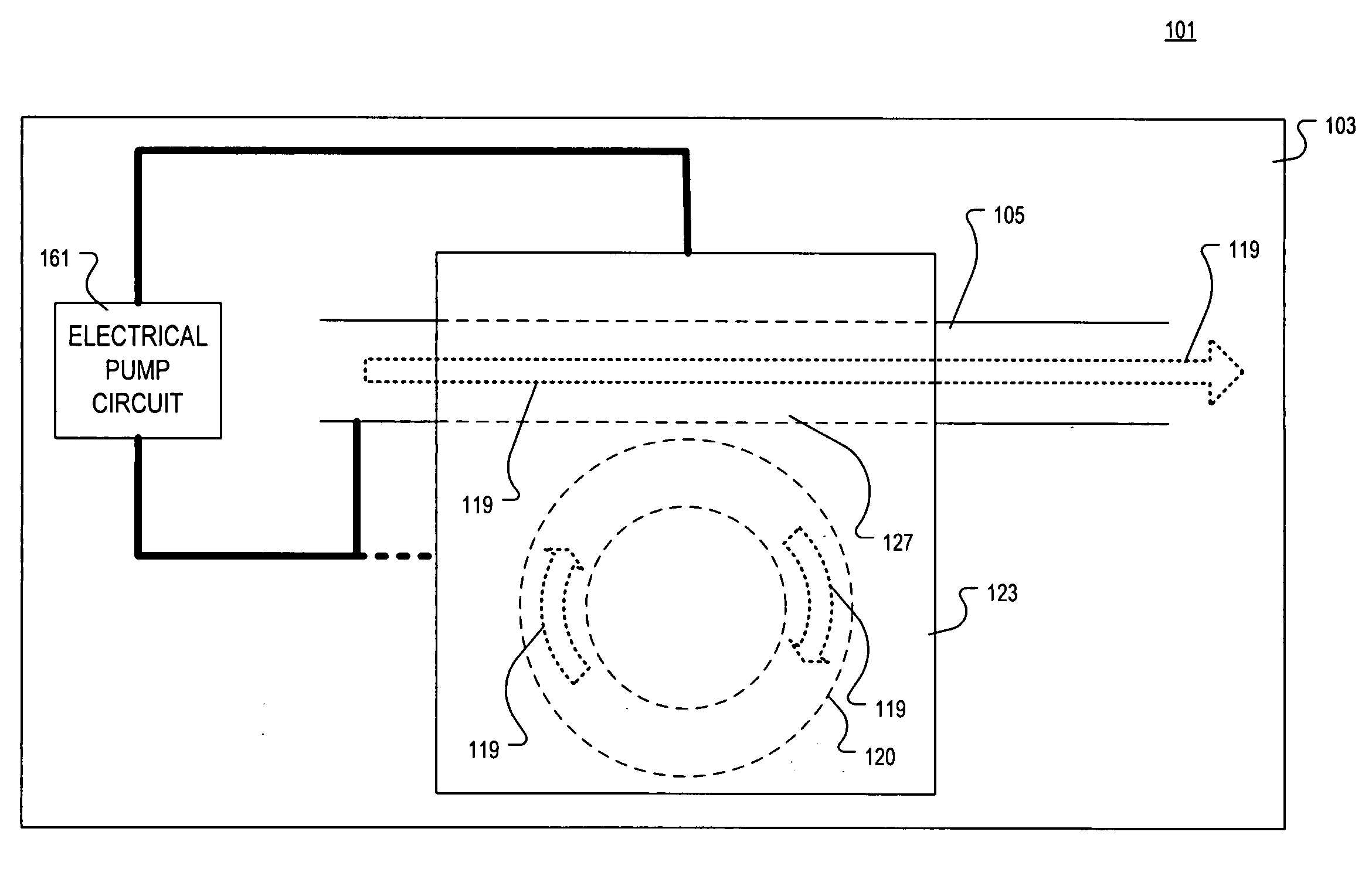
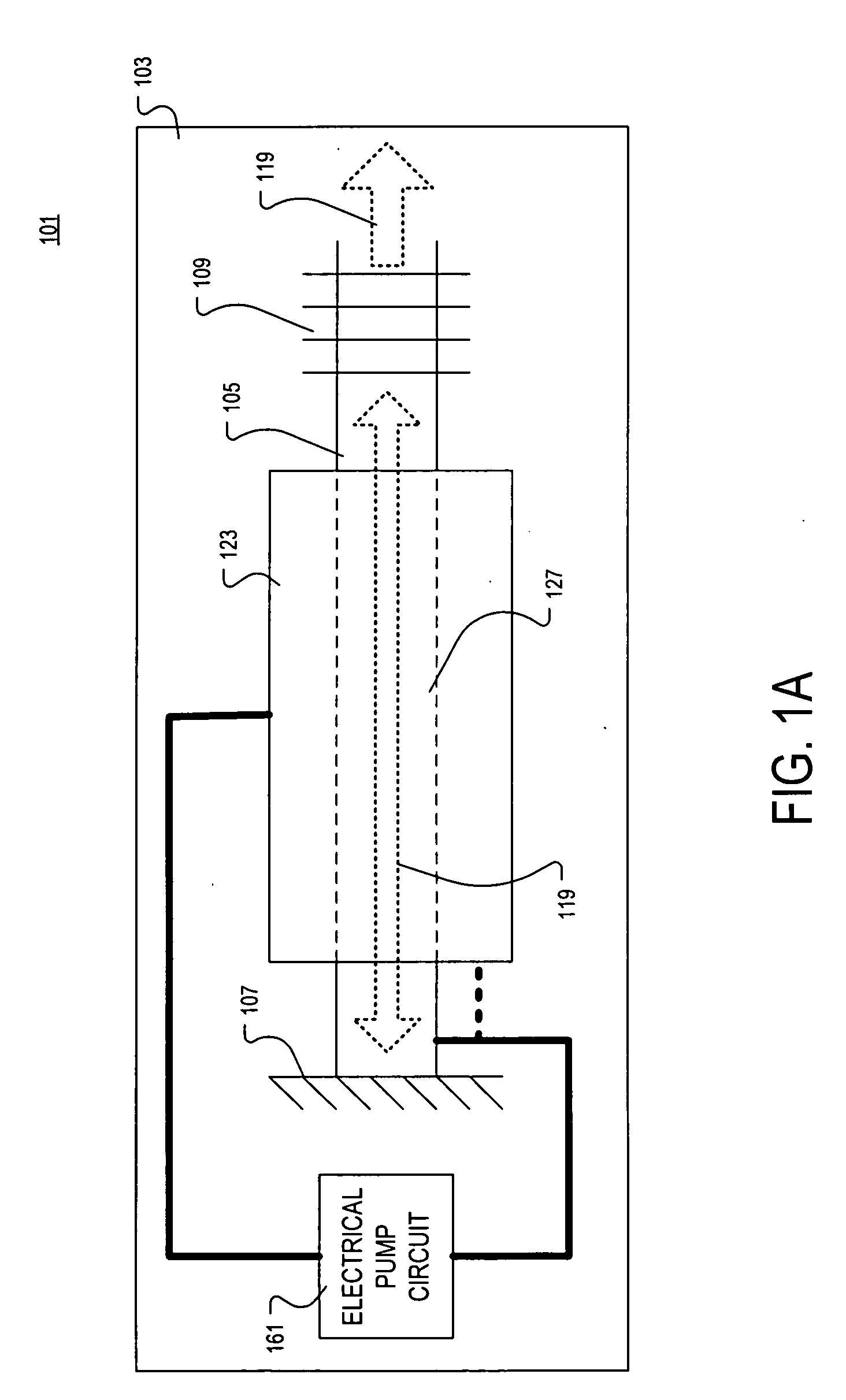
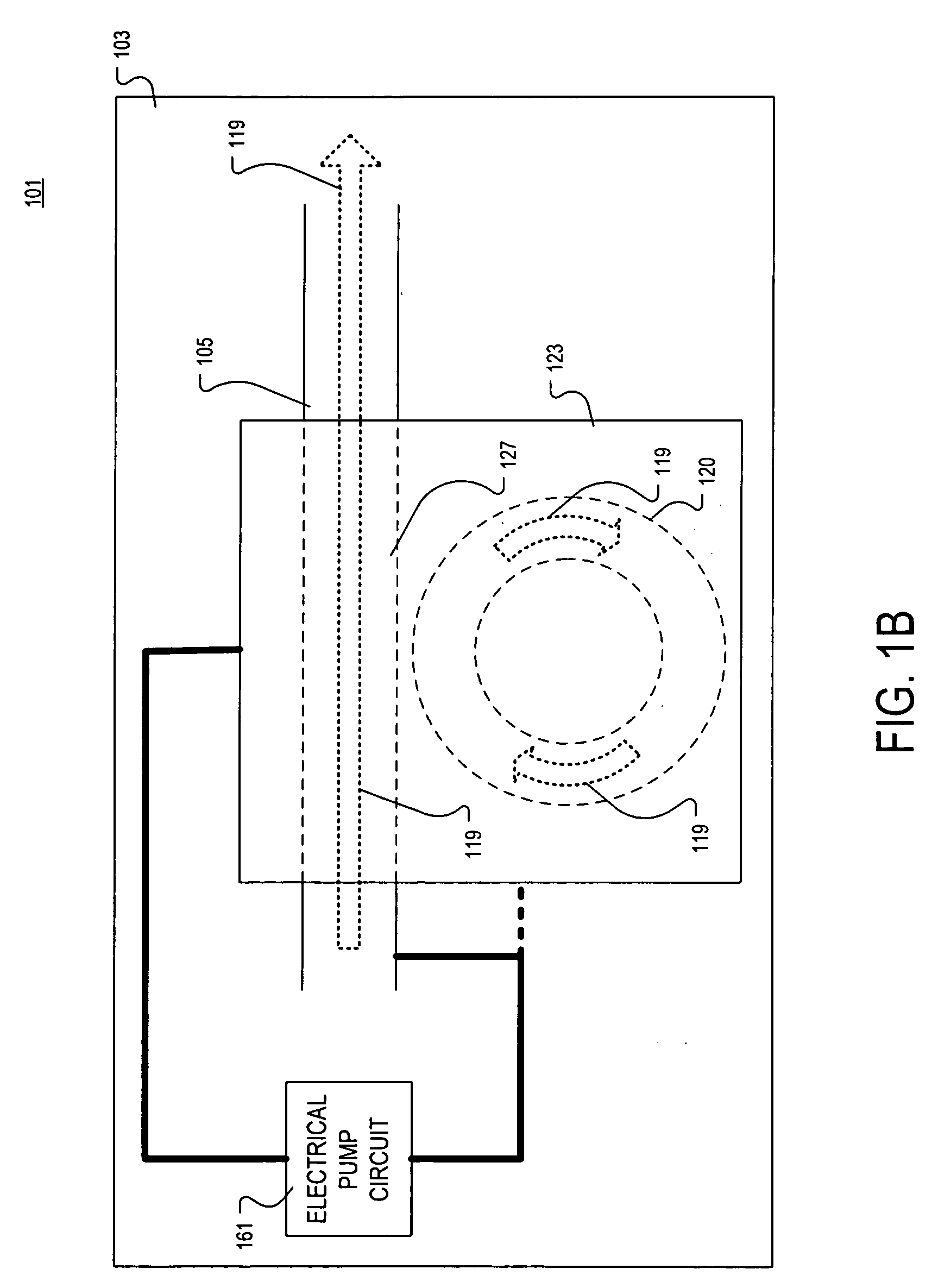
[0021]Methods and apparatuses for providing an electrically pumped hybrid semiconductor evanescent laser array are disclosed. In the following description numerous specific details are set forth in order to provide a thorough understanding of the present invention. It will be apparent, however, to one having ordinary skill in the art that the specific detail need not be employed to practice the present invention. In other instances, well-known materials or methods have not been described in detail in order to avoid obscuring the present invention.

[0022]Reference throughout this specification to “one embodiment” or “an embodiment” means that a particular feature, structure or characteristic described in connection with the embodiment is included in at least one embodiment of the present invention. Thus, appearances of the phrases “in one embodiment” or “in an embodiment” in various places throughout this specification are not necessarily all referring to the same embodiment. Furtherm...


PUM


Abstract

An apparatus and method electrically pumping a hybrid evanescent laser. For one example, an apparatus includes an optical waveguide disposed in silicon. An active semiconductor material is disposed over the optical waveguide defining an evanescent coupling interface between the optical waveguide and the active semiconductor material such that an optical mode to be guided by the optical waveguide overlaps both the optical waveguide and the active semiconductor material. A current injection path is defined through the active semiconductor material and at least partially overlapping the optical mode such that light is generated in response to electrical pumping of the active semiconductor material in response to current injection along the current injection path at least partially overlapping the optical mode.

Description

STATEMENT REGARDING FEDERALLY SPONSORED RESEARCH AND DEVELOPMENT[0001]This invention was made with Government support under Contract No. W911NF-05-1-0175, awarded by the Department of Defense. The Government has certain rights in this invention.BACKGROUND OF THE DISCLOSURE[0002]1. Field of the Invention[0003]The present invention relates generally to optics and, more specifically, the present invention relates to optical interconnects and communications.[0004]2. Background Information[0005]The need for fast and efficient optical-based technologies is increasing as Internet data traffic growth rate is overtaking voice traffic pushing the need for fiber optical communications. Transmission of multiple optical channels over the same fiber in the dense wavelength-division multiplexing (DWDM) systems and Gigabit (GB) Ethernet systems provide a simple way to use the unprecedented capacity (signal bandwidth) offered by fiber optics. Commonly used optical components in the system include wa...

Claims


Application Information

Patent Timeline
IPC IPC(8): G02B6/12G02B6/26H01S3/097
CPCG02B2006/12121H01S5/021H01S5/026H01S5/0424H01S5/0425H01S5/34H01S5/125H01S5/141H01S5/2214H01S5/223H01S5/30H01S5/1032H01S5/04256H01S5/04257H01S5/04H01S5/10
Inventor BOWERS, JOHN E.COHEN, ODEDFANG, ALEXANDER W.JONES, RICHARDPANICCIA, MARIO J.PARK, HYUNDAI
Owner INTEL CORP
Why Eureka
Try Eureka