
Photo-masks and methods of fabricating surface-relief grating diffractive devices

a diffractive device and surface relief technology, applied in the field of optical grating diffractive devices, can solve the problems of high labor intensity, high cost and labor intensity of current processes employed in their manufacture, and the inability to produce such optical components in large quantities, so as to reduce cost and labor.

Inactive Publication Date: 2008-01-03
GEORGIA TECH RES CORP
View PDF10 Cites 24 Cited by
  • Summary
  • Abstract
  • Description
  • Claims
  • Application Information

AI Technical Summary

Benefits of technology

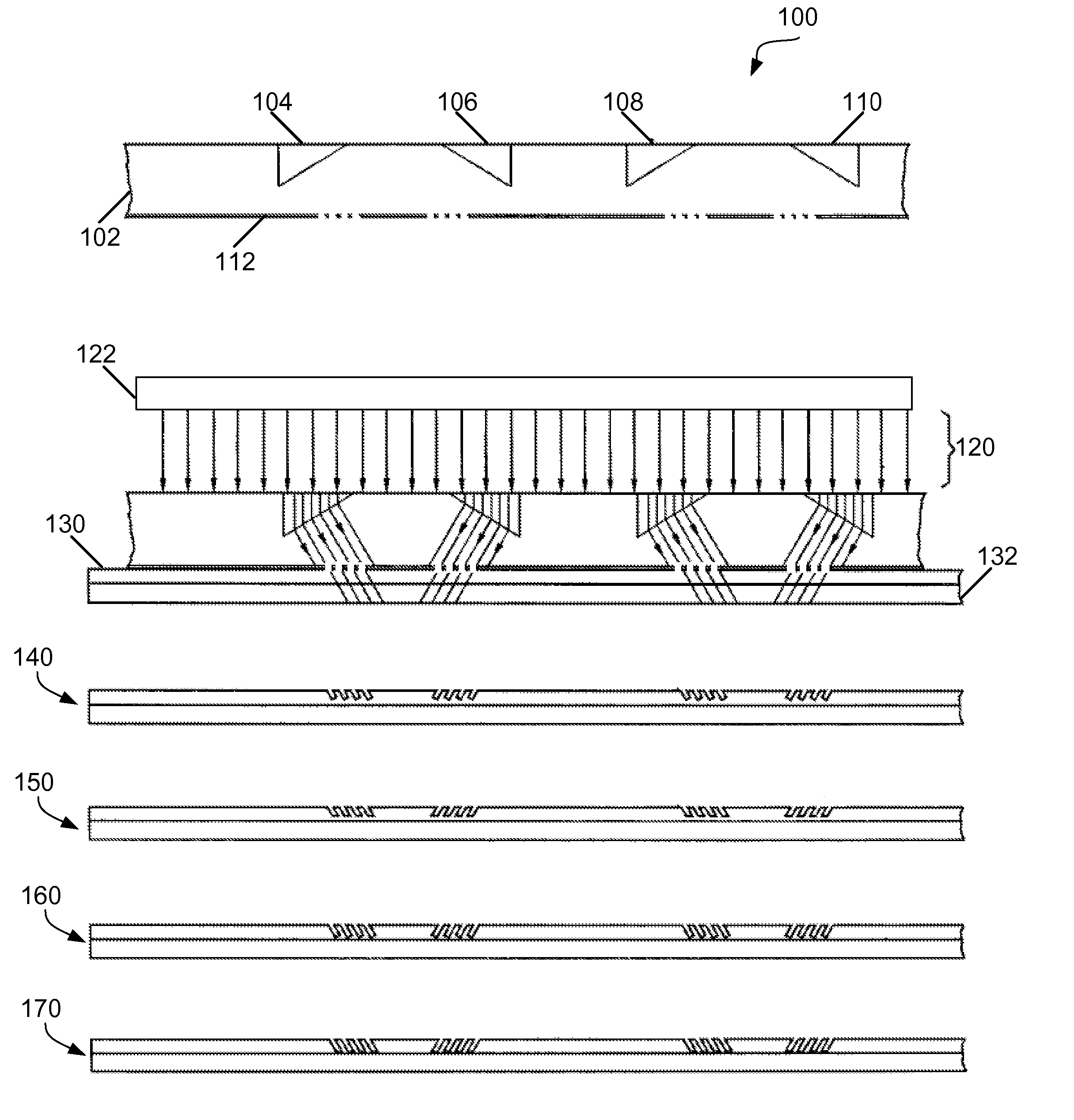
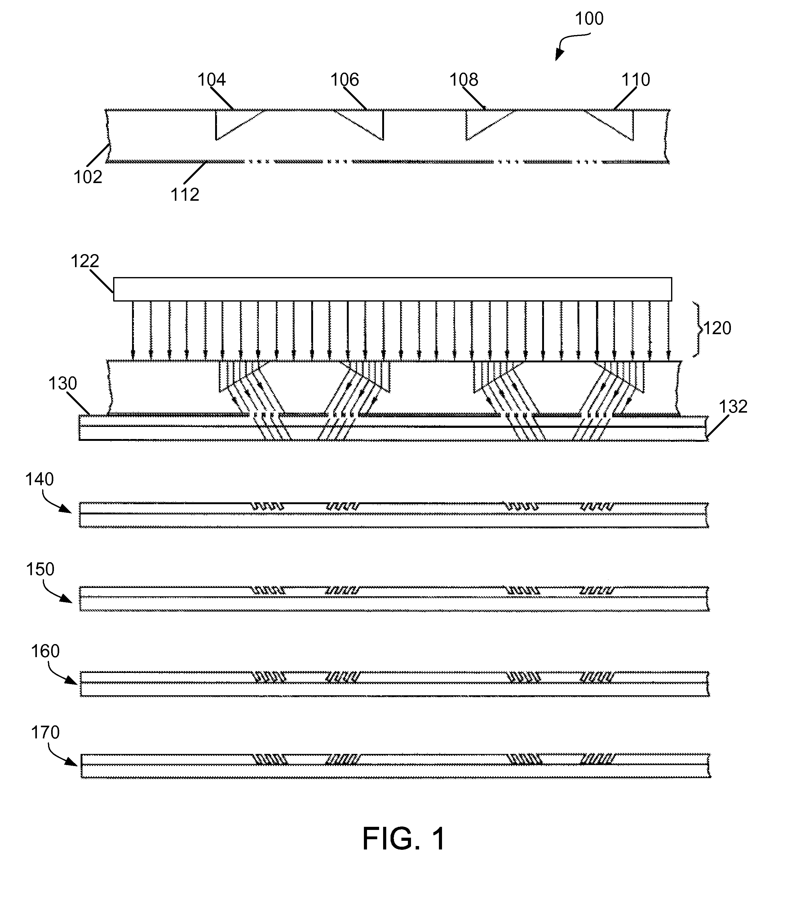
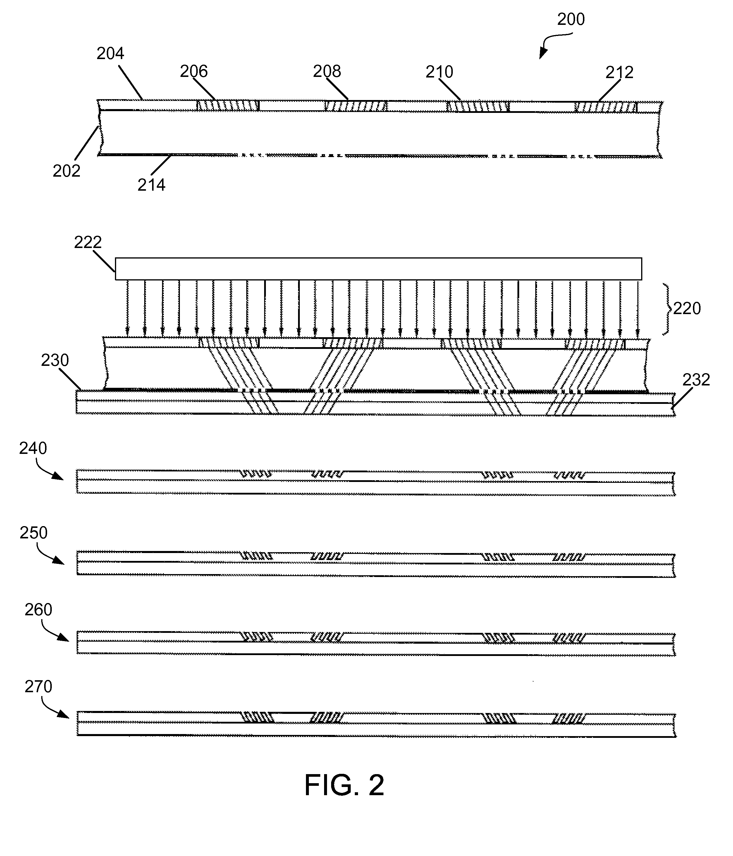
[0009] Broadly described, a photo-mask according to an embodiment of the present invention can include one or both of refractive elements or diffractive elements contained in a substrate or body element of the photo-mask. The diffractive elements can include one or more volume gratings or surface-relief gratings. The refractive elements can include one or more materials having a different index of refraction than the body element. The photo-mask can be used to simultaneously produce multiple surface-relief gratings on a recording material, such as a wafer material. The photo-masks enable the surface-relief couplers to be produced in large quantities while significantly reducing the cost and labor required.

Problems solved by technology

The creation of such optical components has become a time consuming and expensive proposition.
Due to the size of optical waveguides and optical circuitry and other factors, current processes employed in their manufacture can be very costly and labor intensive.
Positioning of such a lens is quite labor intensive, as are the subsequent steps of packaging the overall device, translating into a very high cost.
This high cost impedes the overall creation of optical communications systems.

Method used


Image

  • Photo-masks and methods of fabricating surface-relief grating diffractive devices
  • Photo-masks and methods of fabricating surface-relief grating diffractive devices
  • Photo-masks and methods of fabricating surface-relief grating diffractive devices

Examples


examples

[0047] In this example, a combination of rigorous coupled wave analysis (RCWA) and simulated annealing (SA) were used to determine optimized parallel-face slanted surface-relief gratings (PFSSRGs) in a polymer and in silicon.

[0048] The design technique involved a coarse mapping simulation, followed by localized investigation with an SA algorithm, both steps using RCWA. For PFSSRGs, the variable parameters included the filling factor (equal at the top and bottom of the groove) F, slant angle ø, and groove depth d, which defined a three-dimensional simulation space. Optimization was performed for polymer and silicon cases and both transverse electrical (TE) and transverse magnetic (TM) polarizations at normal incidence in air with an output angle of 45° for the first diffracted order (−1). The simulated configuration is shown in FIG. 7. For completeness, filling factors ranging from 0.01 to 0.99 and slant angles ranging from 1° to 89° were included. An upper limit of 3 micrometers wa...


PUM

PropertyMeasurementUnit
slant anglesaaaaaaaaaa
grating periodaaaaaaaaaa
output angleaaaaaaaaaa

Abstract

Photo-masks for fabricating surface-relief grating diffractive devices and methods of fabricating surface-relief grating diffractive devices are described. The photo-mask can include refractive elements and / or diffractive elements contained in or on a body element. The photo-mask can be used to simultaneously produce multiple surface-relief grating diffractive devices in a recording material. The photo-mask enables the surface-relief grating diffractive devices to be produced in large quantities while significantly reducing the cost and labor required.

Description

CROSS-REFERENCE TO RELATED APPLICATION [0001] The present application claims the benefit of U.S. Provisional Patent Application Ser. No. 60 / 816,278, filed 22 Jun. 2006, and entitled “Phase Masks For Wafer-Scale Fabrication of Surface-Relief Diffractive Couplers,” which is hereby incorporated by reference in its entirety as if fully set forth below.TECHNICAL FIELD [0002] The various embodiments of the present invention relate generally to optical grating diffractive devices (e.g., couplers, feedback devices, sensor devices, and the like), and more particularly, to photo-masks for use in fabricating surface-relief grating diffractive devices, and to methods of making the surface-relief grating diffractive devices. BACKGROUND [0003] Chip-level communication systems are being stressed due to the ever-increasing demand for greater bandwidths to handle evolving interconnection needs. More and more, interconnection systems are evolving to meet these needs by employing optical signaling sys...

Claims


Application Information

Patent Timeline
Patent Type & Authority Applications(United States)
IPC IPC(8): G03C5/56B29D11/00G02B27/42G02B27/44
CPCG02B27/4238G02B5/1857
Inventor GAYLORD, THOMAS K.STAY, JUSTIN L.MAIKISCH, JONATHAN S.MEINDL, JAMES D.
Owner GEORGIA TECH RES CORP
Learn More