S&P2 CWW1 connector with wipe

a technology of electrical connectors and wipes, applied in the direction of fixed connections, coupling device connections, instruments, etc., can solve the problems of increasing the cost of manufacturers, working with many products now available, and increasing the cost of testing devices through more expensive means, so as to reduce the drawbacks, reduce the ill effect of thermal cycling, and small area or footprint

Inactive Publication Date: 2008-01-03
CHERIAN GABE
View PDF6 Cites 29 Cited by
  • Summary
  • Abstract
  • Description
  • Claims
  • Application Information

AI Technical Summary

Benefits of technology

[0042] The object of the invention is to utilize new systems to design and mount springs or needles to reduce the drawbacks that exist in present probes and sockets. This method can be used for probes, sockets, test heads and other interconnections. The basic goal is to provide contact springs that can be located on small, effective center distances to correspond to the center distances of contact pads on chips, wafers, packages, substrates or boards and similar devices. This should also cover a small area or footprint of the devices. Another general goal is to provide a way to support and guide the springs or needles, and to locate them precisely, especially at their tips, where they contact the device under test (DUT). This will reduce the chance of deforming the springs or needles out of position and keeps the tips in close alignment. One more goal is to provide adequate wipe or scrub action at the tips of the springs or needles, thus requiring small forces to break through the undesirable layers on top of the contact pads. Yet another goal is to reduce the ill effect of thermal cycling through the use of TCE-matched combs. Another important goal is to shield the needles and / or make them with controlled impedance to perform like coaxial cables. This would be accomplished by providing an insulating cover, layered over the needles, and then providing another layer of conductive material that can be grounded.

Problems solved by technology

A resulting problem is that sockets, probes and the like are too large, or have their contact elements too large, to work with many of the products which are now available.
This results in increased cost to the manufacturers, who must test the devices through more expensive means.

Method used


Image

  • S&P2 CWW1 connector with wipe
  • S&P2 CWW1 connector with wipe
  • S&P2 CWW1 connector with wipe

Examples


application example 1

[0092]FIG. 5 shows an example of a “socket” built according to the concepts covered here, specifically using the staggered spring arrangement.

[0093] The contact springs are located inside a housing. The housing includes the upper and lower “combs” and the housing body. Depending on the application, the socket may also have a lid to push down on the DUT, a latch to hold the lid down, and other peripheral components. An example of these components is shown in FIG. 32 and will be described later.

[0094]FIG. 7 shows an isometric view of the springs shown in FIG. 5, but without the housing, for clarity's purpose.

[0095] Let us also agree on the coordinate directions. If we look at the socket or the spring matrix from the top, then we will say that this is the x- and y-directions. If we look at the side view, as in FIG. 5, then the horizontal direction is the x-direction, while the vertical direction is the z-direction.

[0096] The 3-Dimensional view in FIG. 7 shows all three directions. ...

illustration example

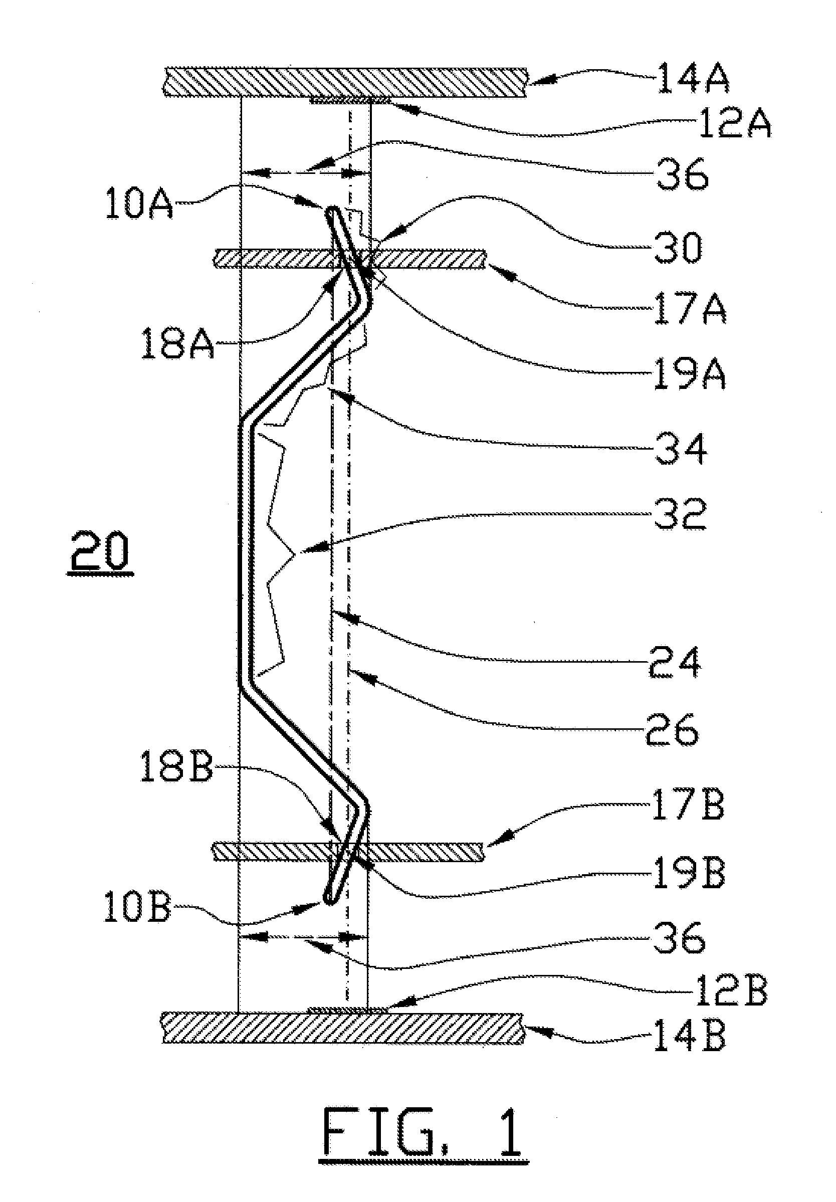
[0121]FIG. 9 is an illustration of parallel nested springs. In this case, the springs are “C”-shaped. They are shown under No-Load, i.e. with no deflection.

[0122]FIG. 10 shows the same springs, but under some load. The natural tendency of such springs, when compressed by an axial load, is to deform as shown. Their bellies have bulged, but because they are all parallel and nested in the same direction, they still do not touch. The tails of the springs tilt when compressed, as shown. Please notice the somewhat slanted hourglass shape of the holes in the top and bottom combs. This shape does not “fight” the natural tendency of the springs tails to rotate or tilt.

[0123] Wipe or Scrub

[0124] Assuming that the device under test (DUT) to be contacted by these springs is “fixed” horizontally or “guided” with respect to the combs, then the compression of the springs creates a horizontal relative motion between the spring tips and the contact pads of the DUT. This relative motion creates a ...

application example 2

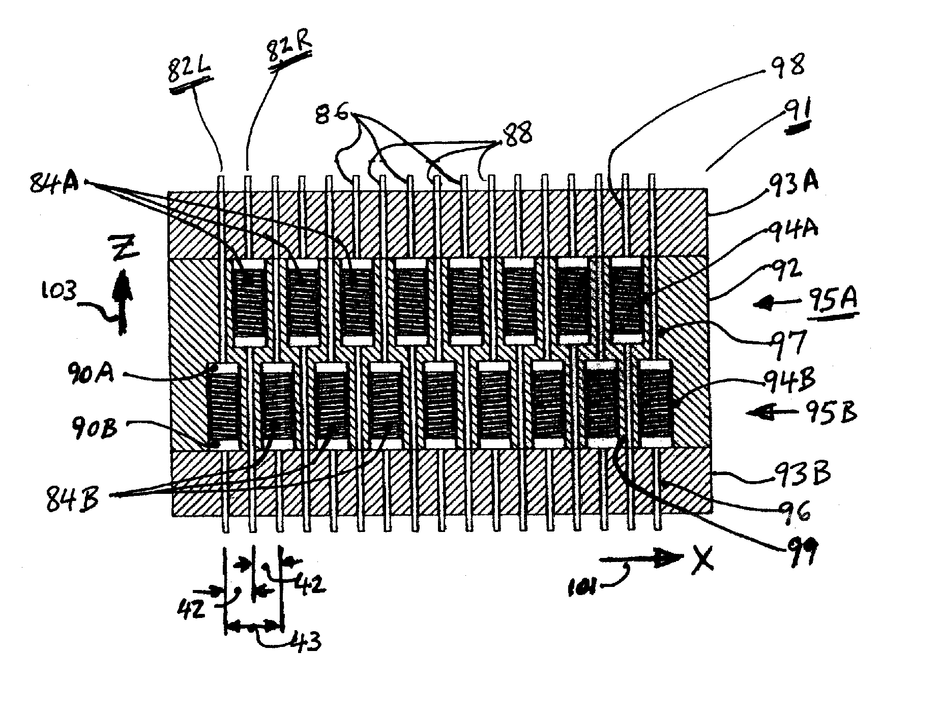
[0127]FIGS. 11 and 12 show a socket implementation containing a matrix of 20 by 20 “C” springs. We are looking at a side view in the x-z directions. This shows only one row of 20 springs. The other rows are behind and are hidden.

[0128]FIGS. 21 through 24 and 30 and 31 show the top view of similar sockets, showing the full matrix.

[0129]FIG. 21 and 31 shows the top view of the socket, with the 20 rows, each having 20 springs.

[0130] The springs are shown in a “parallel nesting” arrangement, held in place with two combs. We also see a middle member.

[0131] The middle member in FIGS. 11 and 12, called a “slider”, moves back and forth with the movement of the bellies of the springs. The springs can slide and move freely through the holes of the slider, as well as through the holes of the top and bottom combs.

[0132] The slider has a number of functions. First, it keeps the springs “organized”. Second, it helps to prevent the springs from touching each other and “shorting. Third, it has...


PUM

PropertyMeasurementUnit
angleaaaaaaaaaa
nesting angleaaaaaaaaaa
center distanceaaaaaaaaaa

Abstract

The present invention relates generally to interconnections between electronic devices, such as integrated circuit packages, chips, wafers, substrates or printed circuit boards or similar electronic devices. The invention relates more specifically to springs or equivalent means, used to make connections to electrical elements and to applications of such springs in connectors or interconnection devices. More particularly the springs or equivalent means can be located adjacent to each other on small effective center distances to accommodate high-density electronic devices. Furthermore, the present invention relates to combs that are used in conjunction with such springs or equivalent means, to create and to control the wiping or scrubbing action, which can promote good electrical connection. Moreover, the present invention uses such combs that are thermally matched to the electronic devices to improve the performance during thermal cycling procedures.

Description

BACKGROUND OF THE INVENTION [0001] 1. Field of the Invention [0002] The present invention generally relates to electrical connectors, and more particularly relates to high-density electrical connectors used in test and burn-in done on miniaturized electrical components. [0003] This invention is a technology platform that enables the interconnection between high-density electronic devices. It first covers the springs and spring arrangements that represent the modular building block of devices to achieve high density interconnection and finally covers several applications utilizing the said springs and arrangements, such as sockets, connectors, probes, test heads and the like. [0004] The invention also relates to combs, which are used in conjunction with said springs, and which promote and control wipe or scrub, and which are thermally matched to the electronic devices, to enhance life and performance especially during thermal cycling procedures. [0005] 2. Background Information [0006...

Claims


Application Information

Patent Timeline
Patent Type & Authority Applications(United States)
IPC IPC(8): H01R13/00H01L23/495H01L23/498H05K3/34
CPCG01R1/0466Y10T29/49218H01L23/49555H01L23/49811H01L2924/3011H01R13/2421H01R13/2435H05K7/1069H01R12/52H01R12/714G01R1/07357Y10T29/49222Y10T29/49204Y10T29/49208H01L2924/00013H01R12/89H01L2924/0002Y10T29/49151Y10T29/49147H01L2224/29099H01L2924/00G01R1/06733
Inventor CHERIAN, GABE
Owner CHERIAN GABE
Why Eureka
Try Eureka