Cluster-Free Amorphous Silicon Film, and Method and Apparatus for Producing the Same

a technology of amorphous silicon and amorphous silicon, which is applied in the direction of silicon compounds, sustainable manufacturing/processing, and final product manufacturing, etc., can solve the problem of light-induced degradation in a-si:h thin film deposited at a high rate, which is a long-standing major problem to be solved, and achieve the effect of lowering the film-deposition ra

Inactive Publication Date: 2008-01-10
KYUSHU UNIV
View PDF0 Cites 11 Cited by
  • Summary
  • Abstract
  • Description
  • Claims
  • Application Information

AI Technical Summary

Benefits of technology

[0019] The cluster-free a-Si:H film of the present invention has prominent characteristics which are not an extension of those of the conventional Si cluster-reduced a-Si:H film, and can eliminate 90% or more of large clusters which have existed in the conventional a-Si:H film, by low-cost means without lowering a film-deposition rate.

Problems solved by technology

While the solar cell using an a-Si:H thin film is expected as a core of power-generating solar cells, light-induced degradation in an a-Si:H thin film deposited at a high rate remains as a long-standing major problem to be solved.

Method used


Image

  • Cluster-Free Amorphous Silicon Film, and Method and Apparatus for Producing the Same
  • Cluster-Free Amorphous Silicon Film, and Method and Apparatus for Producing the Same
  • Cluster-Free Amorphous Silicon Film, and Method and Apparatus for Producing the Same

Examples


first embodiment

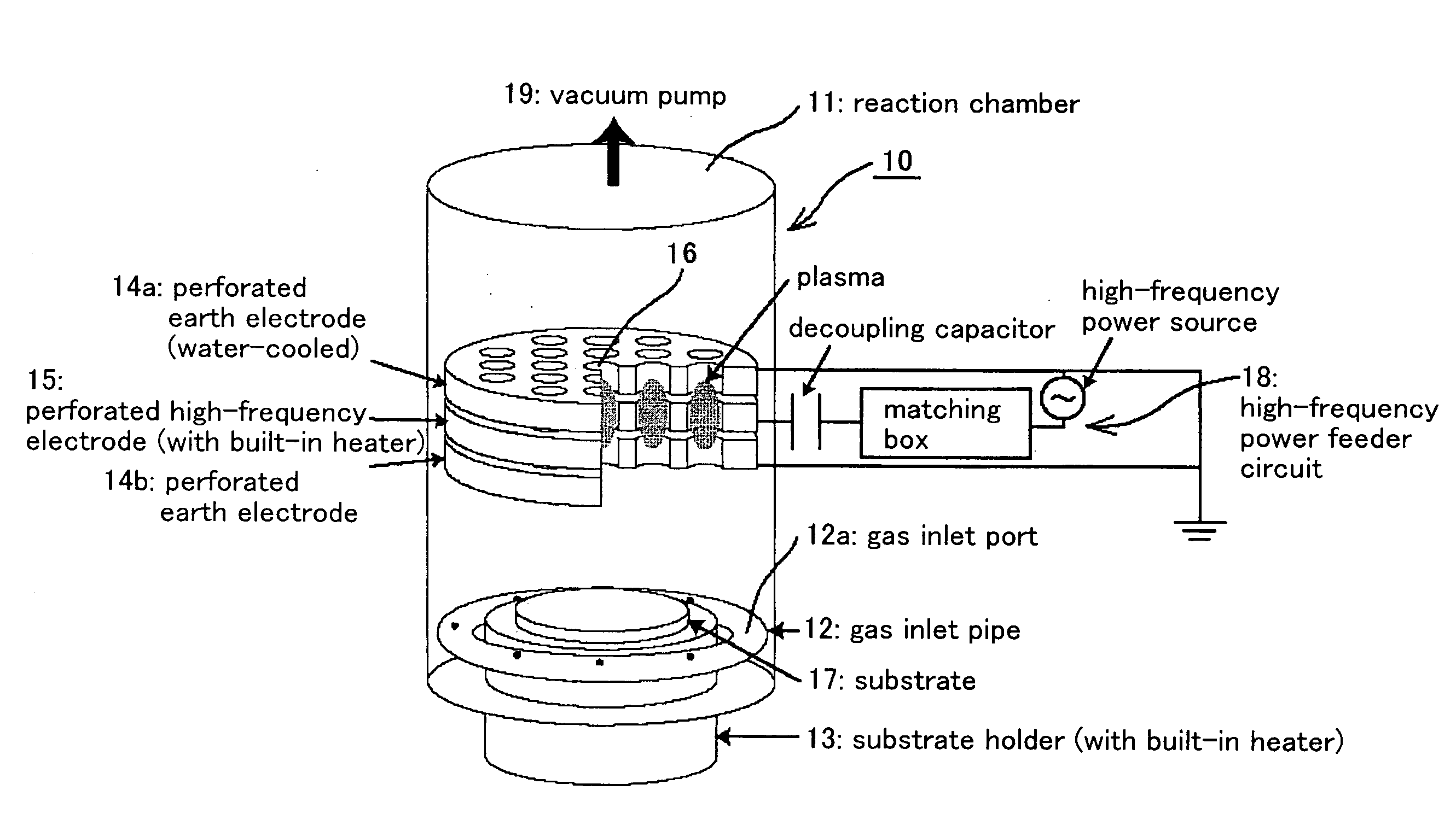
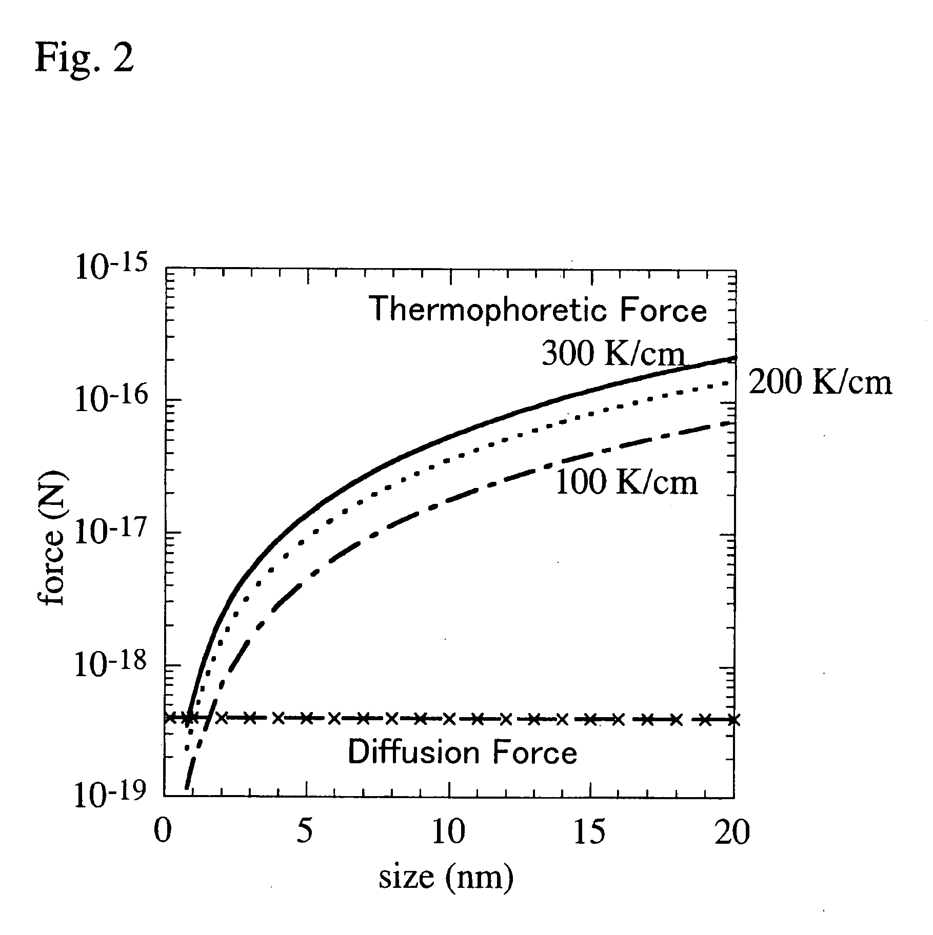
[0021] In a first embodiment of the present invention, a technique of increasing a gas flow rate in a plasma region, generating a thermophoretic force which acts on large clusters in gaseous phase, and capturing large clusters by an inner wall of a hole to remove the large clusters is used for preventing the incorporation of large clusters in an a-Si:H film to be deposited. FIG. 1 shows an amorphous silicon thin film deposition apparatus 10 (hereinafter referred to simply as apparatus 10″) using the above technique. As shown in FIG. 1, the apparatus 10 comprises a cylindrical-shaped reaction chamber (vacuum chamber) 11, a substrate holder 13 attached to a bottom of the reaction chamber 11 and provided with a gas inlet pipe 12, and a vacuum pump 19 connected to a top of the reaction chamber 11. A pair of perforated earth electrodes 14a, 14b and a perforated high-frequency electrode 15 are disposed parallel to each other within the reaction chamber 11, and a gas is directed to flow in...

second embodiment

[0030] In a second embodiment of the present invention, a cluster removal filter is used as one of large-cluster removal means. FIG. 7 shows an amorphous silicon thin film deposition apparatus 20 (hereinafter referred to simply as “apparatus 20”) using a cluster removal filter 21 as one of the large-cluster removal means. In this apparatus 20, a mesh-shaped high-frequency electrode 22, a mesh-shaped earth electrode 23 and a substrate 24 are disposed in a face-to-face arrangement within a reaction chamber (vacuum chamber) 25, and the cluster removal filter 21 is arranged immediately below the earth electrode 23. The mesh-shaped high-frequency electrode 22 and the mesh-shaped earth electrode 23 are disposed parallel to each other, and gas is directed to flow in a direction perpendicular to each surface of the electrodes. The substrate 24 may be made of Si, glass, stainless steel or polymer.

[0031] As shown in FIG. 7, the cluster removal filter 21 is arranged in a space through which a...

third embodiment

[0035] In a third embodiment of the present invention, a gas curtain (high-speed silane gas flow) is used as one of the large-cluster removal means, and employed in an amorphous silicon thin film deposition apparatus 30 (hereinafter referred to simply as “apparatus 30”) illustrated in FIG. 9 to produce a cluster-free a-Si:H film of the present invention. The apparatus 30 illustrated in FIG. 9 comprises a reaction chamber (vacuum chamber) 31 which houses a high-frequency electrode 32, an earth electrode 33 provided with a built-in heater and disposed in vertically opposed relation to the high-frequency electrode 32, and a substrate 34 adapted to allow an a-Si:H thin film to be deposited thereon and placed on the earth electrode 33. The apparatus 30 is designed to feed a high-frequency power generated by a high-frequency power feeder circuit (not shown) to the high-frequency electrode 32 to create a plasma in a silane gas introduced between the high-frequency electrode 32 and the eart...


PUM

PropertyMeasurementUnit
volume fractionaaaaaaaaaa
sizeaaaaaaaaaa
sizeaaaaaaaaaa

Abstract

The intention is to clarify characteristics of a cluster-free amorphous silicon film which is practically produceable without incorporation of large clusters having a size of 1 nm or more, and provide a method and an apparatus for producing the amorphous silicon film. In the cluster-free amorphous silicone (a-Si:H) film, an in-film Si—H2 bond density is 10−2 atomic % or less, and an in-film volume fraction of the large clusters is 10−1% or less. The a-Si:H film is produced by depositing, on a substrate, a deposition material in a plasma flow of any one of a silane gas, a disilane gas and a gas obtained by diluting a silane or disilane gas with one or a combination of two or more selected from the group consisting of hydrogen, Ar, He, Ne and Xe. The a-Si:H film has prominent characteristics, such that: a light-induced defect density is reduced from 2×1016 cm−3 or more in conventional a-Si:H films to substantially zero; a stabilized efficiency (%), i.e., a light-energy conversion efficiency, is increased from 9% at the highest in existing a-Si:H films up to 14% or more; and a light-induced degradation rate, i.e., [(initial efficiency−stabilized efficiency) / initial efficiency]×100%, is reduced from 20% at the lowest in the existing a-Si:H films to substantially zero.

Description

TECHNICAL FIELD [0001] The present invention relates to a cluster-free amorphous silicon film which is free from large clusters having a size of 1 nm or more, and the production of the amorphous silicon film. BACKGROUND ART [0002] It is the highest priority issue in the 21st century to solve problems of expanding energy consumption and environmental destruction arising from economic development and population growth (so-called “trilemma”). Photovoltaic power generation is expected to play a large role in solving the problems, and therefore solar cells are needed to achieve higher efficiency and lower cost. [0003] Heretofore, an amorphous silicon (hereinafter referred to as “a-Si:H”) thin film for use in a photoelectric conversion element for solar cells has been deposited, for example, in the following manner. A pair of flat-plate electrodes are disposed parallel to each other in a vacuum vessel, and a substrate is held by one of the flat-plate electrodes. After a silane gas is supp...

Claims


Application Information

Patent Timeline
Patent Type & Authority Applications(United States)
IPC IPC(8): H01L21/205C01B33/027H01L31/04C23C16/24
CPCC23C16/24C23C16/45502C23C16/509H01L31/03767H01L21/0262Y02E10/50H01L21/0245H01L21/02532H01L31/202Y02P70/50H01L21/205
Inventor WATANABE, YUKIOSHIRATANI, MASAHARUKOGA, KAZUNORI
Owner KYUSHU UNIV
Why Eureka
Try Eureka