Display Panel Structure and Manufacture Method Thereof

a technology of display panel and manufacturing method, which is applied in the direction of semiconductor devices, semiconductor/solid-state device details, electrical devices, etc., can solve the problems of increasing display size, reducing the manufacturing process steps, and increasing the display size, so as to achieve good adhesive force and simple manufacturing process steps

Active Publication Date: 2008-01-10
AU OPTRONICS CORP
View PDF1 Cites 32 Cited by
  • Summary
  • Abstract
  • Description
  • Claims
  • Application Information

AI Technical Summary

Benefits of technology

[0010]The other purpose of the present invention is to provide a structure and manufacture method of display panel including simple manufacture process steps.
[0012]The first conductive layer is formed over the first interface layer. The material of the first conductive layer is copper or copper alloy. Besides, the material of the first interface layer at least includes a reactant or a compound formed the first conductive layer. Because the materials of the first interface layer and the first conductive layer have common compositions, only one etching process is used to etch the first interface layer and the first conductive layer at the same time. By disposing the first interface layer, the problem of diffusing the first conductive layer into the substrate can be improved when the first conductive layer is formed. In addition, the existence of the first interface layer is able to enhance the adhesive force between the first conductive layer and the substrate and improve the problem of the first conductive layer peeling off from the substrate.

Problems solved by technology

Because of the fast development of new technology, the principle issue to design the display device is to increase the display size.
Especially in the field of liquid crystal display (LCD) panel, how to increase the display size of the panel is an important issue in the manufacture industries.
When the display size of LCD panel is increased, the conventional impedance made of aluminum or aluminum alloy is too large.
However, the cost of silver is too expensive and it is causing the product made of silver lose its competitiveness in the market industry.
However, there are some limitations and problems by using copper to be the alternative material.
Besides, because the diffusivity of the copper is too large, the copper is easy to penetrate into the substrate when it is deposited onto the substrate, which greatly affects the quality of the LCD.
However, the process of the isolated layer 20 will complicate the whole manufacture process and increase the cost of time and money.
The etching problem of the existing residue will occur and the tolerance percentage of the product will decrease.

Method used


Image

  • Display Panel Structure and Manufacture Method Thereof
  • Display Panel Structure and Manufacture Method Thereof
  • Display Panel Structure and Manufacture Method Thereof

Examples


Embodiment Construction

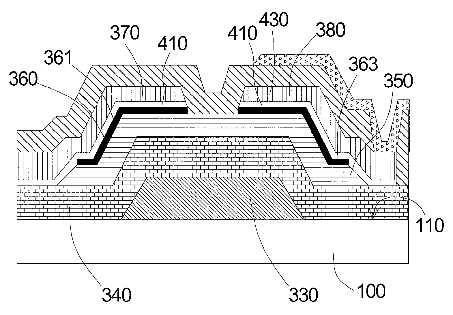
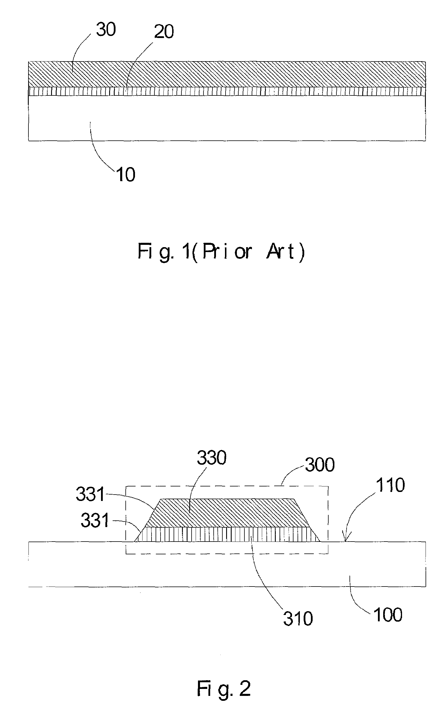
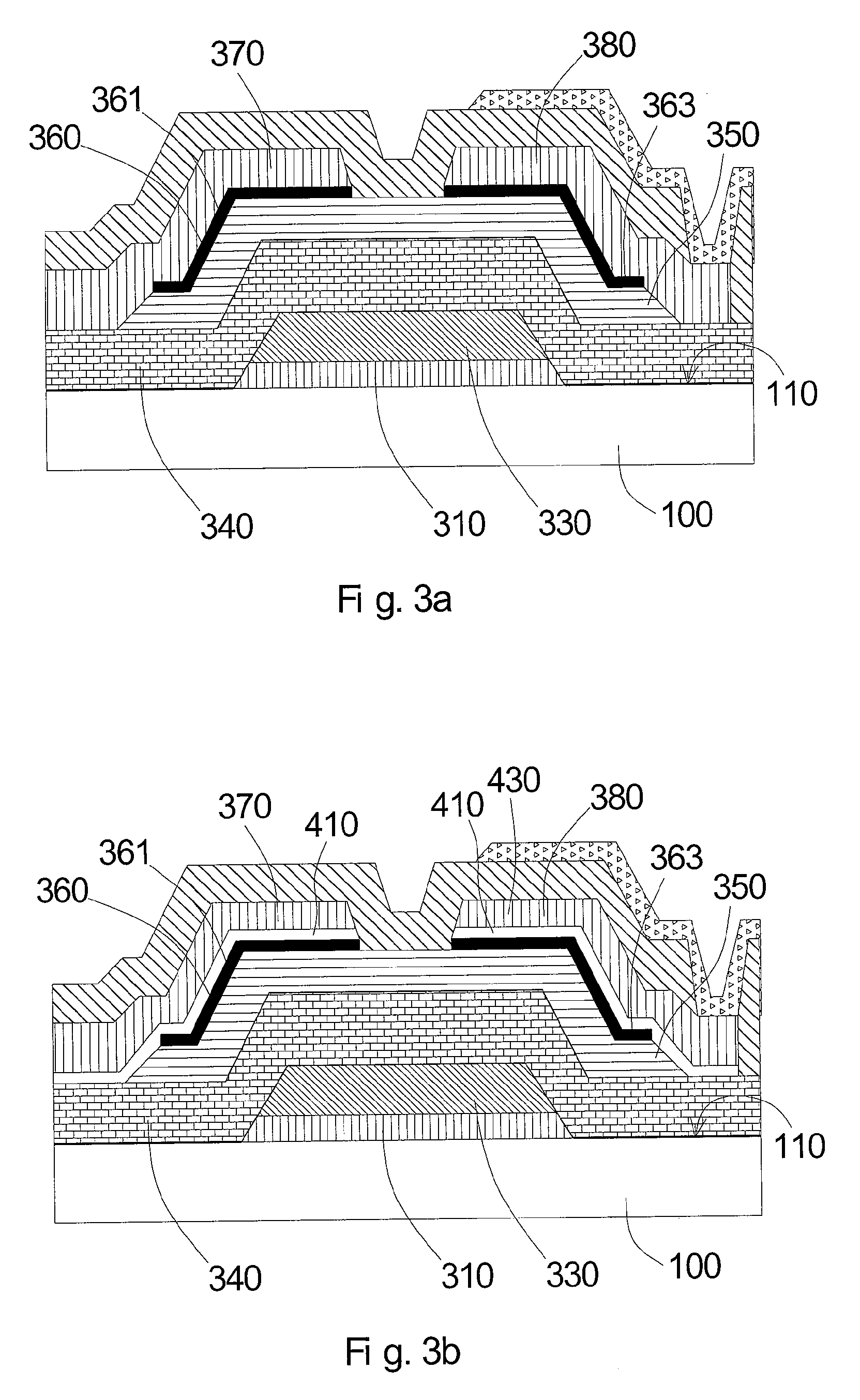
[0027]A structure and manufacture method of display panel is disclosed in the present invention. In the preferred embodiment, the structure of the display panel presented here is a liquid crystal display (LCD) panel. However, in a different embodiment, the structure of the display panel is an organic light emitting diode (OLED) LCD panel or other display device.

[0028]FIG. 2 illustrates an embodiment of the present invention showing a display panel structure. In the embodiment, the display panel structure includes a substrate 100 and a circuit element 300. The substrate 100 is a substrate preferably made of glass. In a different embodiment, the substrate 100 is a substrate made of polymer, such as plastic substrate. Besides, the circuit element 300 includes transistor, such as a-Si thin-film-transistor (a-Si TFT) or p-Si TFT. In a different embodiment, the circuit element 300 is a metal-insulator-metal thin-film-diode (MIM-TFD).

[0029]The circuit element 300 includes a first interface...


PUM


Abstract

A display panel structure having a circuit element disposed thereon and method of manufacture are provided. The display panel includes a substrate and the circuit element disposed on the substrate. The circuit element has a first interface layer and a first conductive layer. Both the first interface layer and the first conductive layer have copper materials. The material which makes the first interface layer includes a reactant or a compound of the material which makes the first conductive layer. The method for manufacturing includes the following steps: forming a first interface layer on the substrate; forming a first conductive layer on the first interface layer; and etching the first conductive and interface layers to form a pattern. The existence of the first interface reduces the penetration of the first conductive layer on the substrate and improves the adhesive force between the first conductive layer and the substrate.

Description

BACKGROUND OF THE INVENTION[0001]1. Field of the Invention[0002]The present invention generally relates to a structure and manufacture method of display panel. More particularly, the present invention relates to a structure and manufacture method of display panel with circuit elements.[0003]2. Description of the Prior Art[0004]By highly developed technology in the modern society, the demand of the video-audio enjoyment for the consumers is increasing day after day. Because of the fast development of new technology, the principle issue to design the display device is to increase the display size. Especially in the field of liquid crystal display (LCD) panel, how to increase the display size of the panel is an important issue in the manufacture industries.[0005]When the display size of LCD panel is increased, the conventional impedance made of aluminum or aluminum alloy is too large. In order to reduce the impedance value, the silver or copper is used to be the alternative material in...

Claims


Application Information

Patent Timeline
Patent Type & Authority Applications(United States)
IPC IPC(8): H01L21/84H01L21/00
CPCH01L29/458H01L29/66765H01L29/66757H01L29/4908
Inventor LIN, CHUN-NANTU, KUO-YUANWU, SHU-FENGTSAI, WEN-CHING
Owner AU OPTRONICS CORP
Why Eureka
Try Eureka