Hot plate and process for producing the same

a technology of hot plate and process, which is applied in the direction of hot plate heating arrangement, ohmic resistance heating, electrical equipment, etc., can solve the problems of non-uniform value distribution of hot plate, affecting the uniformity of semiconductor wafer temperature, and affecting the accuracy of sensing semiconductor wafer temperature, so as to achieve uniform width and thickness, high accuracy, and high accuracy

Inactive Publication Date: 2008-01-17
TOKYO ELECTRON LTD
View PDF8 Cites 54 Cited by
  • Summary
  • Abstract
  • Description
  • Claims
  • Application Information

AI Technical Summary

Benefits of technology

[0010] Under the above-described circumstances, the present invention was accomplished. An object of the present invention is to provide a hot plate comprising a heater improved in uniformity in heating value, capable of more uniformly heating a substrate to be treated, and a process for producing the hot plate.
[0019] According to the present invention, since the heater is made directly on the back surface of the silicon base of the hot plate by MEMS (Micro Electro Mechanical Systems) or a semiconductor production technique, it is more uniform in width and thickness and has higher accuracy as compared with conventional heaters made by printing or bonding. Such a heater of the invention can make the heating value of the hot plate uniform, so that the hot plate can more uniformly heat a substrate, such as a semiconductor wafer, placed on the hot plate.
[0020] Further, in the present invention, since the temperature sensor is also made directly on the back or front surface of the silicon base of the hot plate, its accuracy is high. Therefore, it becomes possible to control precisely the temperature of the hot plate by providing a plurality of the temperature sensors.
[0021] Furthermore, in the present invention, gap pins are made as the gap-making protrusions on the front surface of the silicon base of the hot plate, so that a gap can be accurately made between the hot plate and a substrate placed on the gap-making protrusions.
[0022] Furthermore, in the present invention, since a vacuum holding hole and a vacuum holding groove are made in the front surface of the silicon base of the hot plate, a substrate can be vacuum held and fixed forcedly to the hot plate even if the substrate is curved. The substrate can thus be evenly held on the hot plate. Moreover, since a photolithographic technique and etching are employed to make the a vacuum holding groove and the vacuum holding hole, the groove and the hole have the function of accurately chucking a substrate to vacuum hold it evenly.

Problems solved by technology

It is therefore inevitable that the heater formed on the base plate be non-uniform in width or thickness, which often makes the heating value distribution of the hot plate non-uniform and affects the uniformity in semiconductor wafer temperature.
Further, in the case where temperature sensors are provided on the base plate, they have so far been embedded in or bonded to the base plate, so that they are often not precise in position or non-uniform in size, which affects the accuracy in sensing the semiconductor wafer temperature.

Method used


Image

  • Hot plate and process for producing the same
  • Hot plate and process for producing the same
  • Hot plate and process for producing the same

Examples


first embodiment

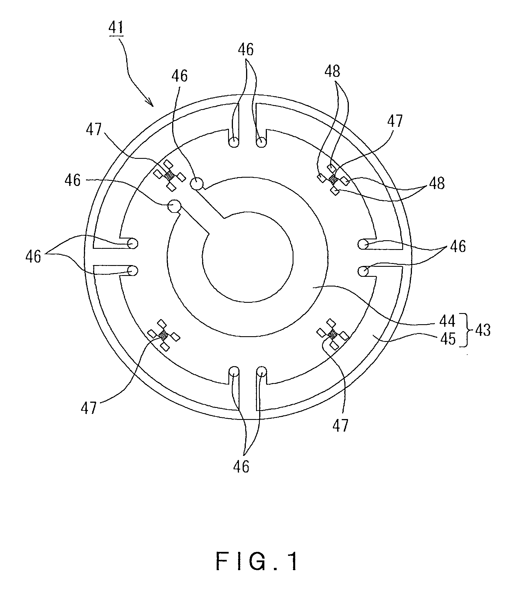
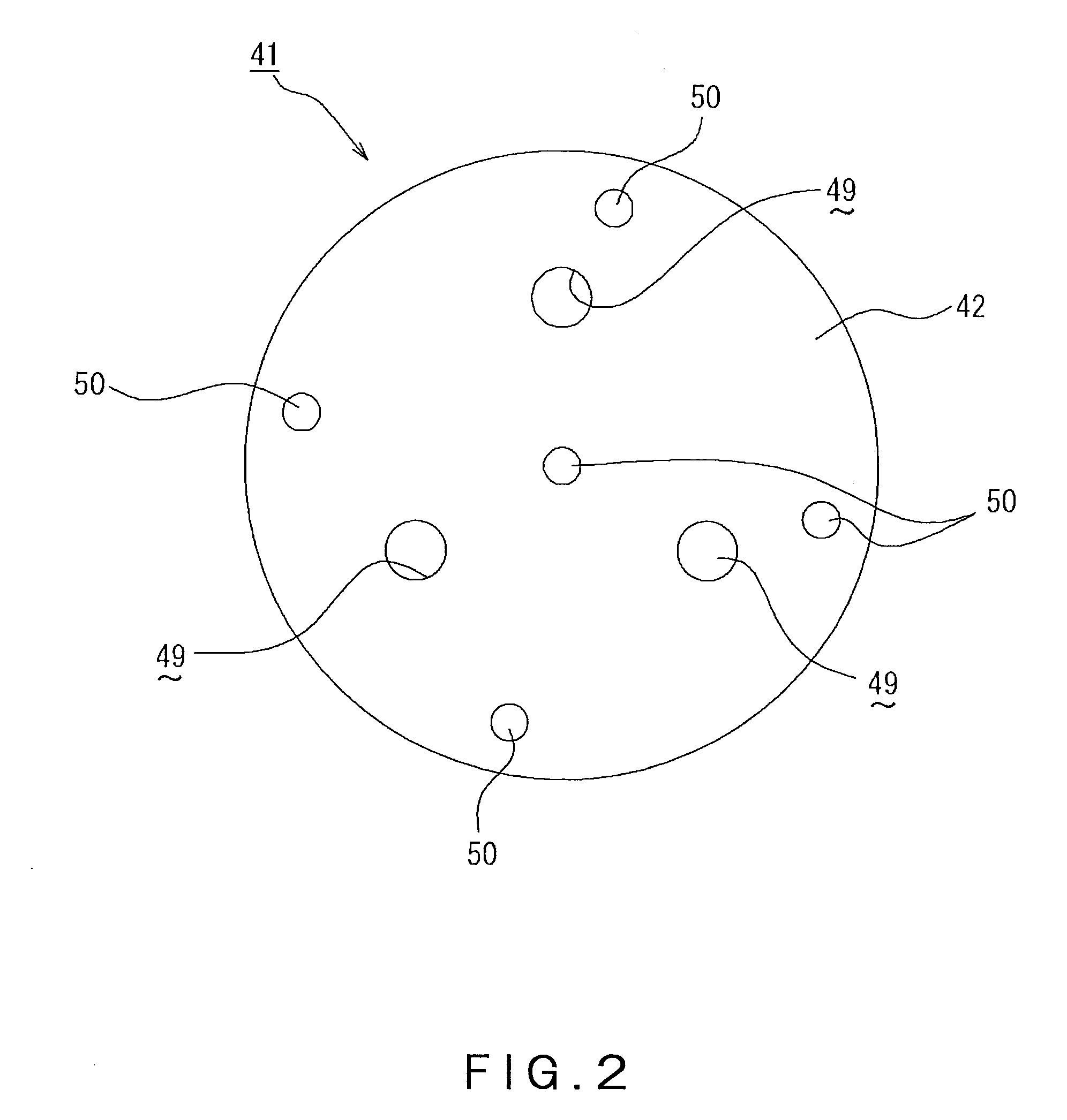
[0042]FIG. 1 is a view showing the back surface of a hot plate 41 useful for heat treatment according to the first embodiment of the present invention, and FIG. 2 is a view showing the front surface of the hot plate 41. The hot plate 41 shown in these figures is intended for a wafer with a thickness of 750 μm and a diameter of 300 mm, for example, and 0.5 to 3-mm thick wafers with a diameter of 340 mm can be placed on it.

[0043] The base plate of this hot plate 41 is a disc-shaped silicon base 42 with a thickness of 0.5 to 3 mm and a diameter of 340 mm, for example, and, on its back surface, a linear or belt-like heater 43 is provided by depositing, by sputtering, a film of platinum (Pt), a resistor, in a predetermined pattern such as a winding pattern, an arc, or a pattern with one stroke, in FIG. 1. In this Specification, the belt-like heater means not only a flat heating element but also a linear heating element that has been zigzagged, for example, to form a plane as a whole.

[0...

second embodiment

[0067]FIG. 9 is a view showing the front surface of a hot plate 41 according to the second embodiment of the present invention.

[0068] In the above-described first embodiment, the gap pins 50 are formed as gap-making protrusions by etching the silicon base 42. In this second embodiment, on the other hand, annular protrusions 75 uniform in thickness are made on the front surface of the silicon base 42 as the gap-making protrusions by the use of a polyimide resin, an insulating synthetic resin material, as shown in FIG. 9. In the case shown in FIG. 9, a first annular protrusion 76 is formed in the center of the silicon base 42, and a second annular protrusion 77, at the edge. These annular protrusions 75 are made in such positions that they do not cross the three pin insertion holes 49.

[0069] In the front surface of the silicon base 42, a vacuum holding hole 78 is made in the center, and vacuum holding grooves 79 are made so that they communicate with the vacuum holding hole 78, in o...

third embodiment

[0077] The third embodiment of the present invention is shown in FIG. 12. In this embodiment, temperature sensors 47 are formed not on the back surface but on the front surface of a silicon base 42. The third embodiment is advantageous in that since the temperature of a wafer W, an object of heating, can be controlled according to the temperature sensed at a point nearer the wafer W as compared with the case where temperature sensors 47 are formed on the back surface of a silicon base 42, the wafer W temperature can be controlled more accurately.

[Procedure for Making Temperature Sensors 47 on the Front Side (FIGS. 13 and 14)]

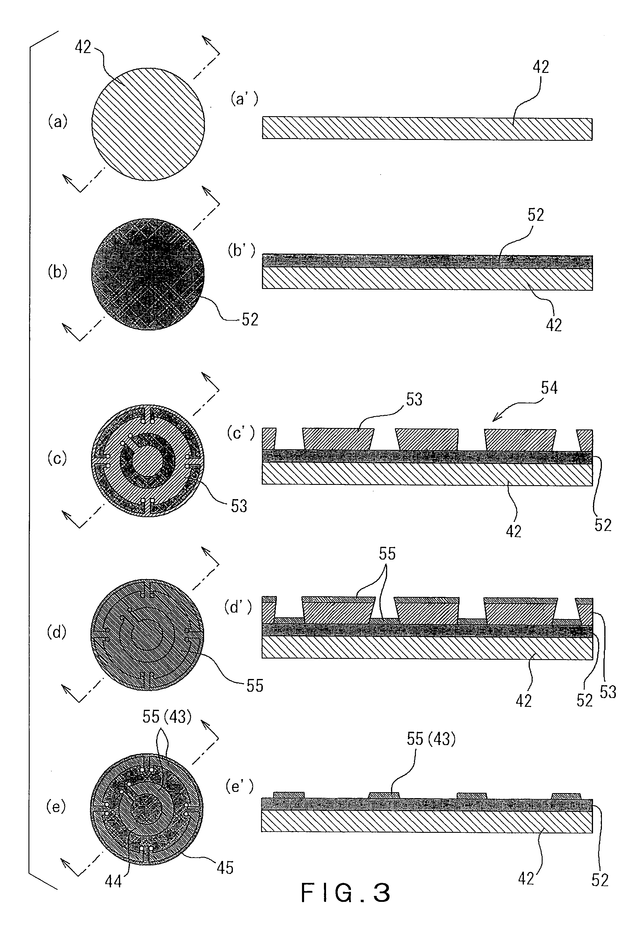
[0078] The procedure for making the temperature sensors 47 on the front surface of the silicon base 42 will be described. This procedure is shown in FIGS. 13 and 14. In FIGS. 13 and 14, views (a) to (g) on the left-hand side show the front surface of the hot plate 41, and views (a′) to (g′) on the right-hand side, a section of the hot plate 41 taken along the ...


PUM

PropertyMeasurementUnit
thicknessaaaaaaaaaa
thicknessaaaaaaaaaa
diameteraaaaaaaaaa

Abstract

A hot plate for heating a substrate placed on the hot plate. The hot plate comprises a silicon base having pin insertion holes through which support pins for supporting a substrate from below and elevating the substrate above the hot plate pass; a heater composed of a resistor made of a metal film deposited on the back surface of the silicon base; and a temperature sensor, composed of a resistor made of a metal film deposited on the back or front surface of the silicon base. The front surface of the silicon base has gap-making protrusions for making a gap between the hot plate and a substrate placed on the gap-making protrusions.

Description

CROSS-REFERENCE TO RELATED APPLICATION [0001] This application claims priority to Japanese Patent Application No. 2006-158898 filed on Jun. 7, 2006, and the whole description in Application No. 2006-158898 is incorporated herein by reference. BACKGROUND OF THE INVENTION [0002] 1. Field of the Invention [0003] The present invention relates to a hot plate for uniformly heating a substrate, such as a semiconductor wafer, to be treated, and to a process for producing it. [0004] 2. Background Art [0005] The process of semiconductor device production includes the steps of thermally treating a wafer on which a semiconductor device will be made. For example, in heat treatment for drying that is carried out after resist coating, in post exposure baking, and in CVD for depositing a predetermined thin film on a semiconductor wafer surface, a table on which a semiconductor wafer is placed is provided with a heater, and, with this heater, the semiconductor wafer on the table is heated to a prede...

Claims


Application Information

Patent Timeline
Patent Type & Authority Applications(United States)
IPC IPC(8): H05B3/68
CPCH01L21/67103Y10T29/49083H05B3/143
Inventor FUKUOKA, TETSUOKITANO, TAKAHIRO
Owner TOKYO ELECTRON LTD
Why Eureka
Try Eureka