Addressable Transistor Chip For Conducting Assays

a technology of conducting assays and transistors, applied in the field of addressable biochips, can solve the problems of ionic shortage of different sensing arrayed electrodes, relatively high manufacturing costs of devices, and high cost of existing biochip technology,

Inactive Publication Date: 2008-01-17
NANYANG TECH UNIV
View PDF5 Cites 143 Cited by
  • Summary
  • Abstract
  • Description
  • Claims
  • Application Information

AI Technical Summary

Benefits of technology

[0007] In accordance with an aspect of the present invention, a bioelectronic microchip includes: a substrate; a plurality of field effect transistors, each including: a first and second electrodes on the substrate; and a channel extending between t

Problems solved by technology

A limiting factor of such MOSFET devices is the relatively high manufacturing costs.
Existing biochip technology is based however on fluorescent-based glass or silicon array fabrication and can be very expensive.
A major obstacle in the development of an addressable electronic array biochip is the occurrence of

Method used


Image

  • Addressable Transistor Chip For Conducting Assays
  • Addressable Transistor Chip For Conducting Assays
  • Addressable Transistor Chip For Conducting Assays

Examples


Embodiment Construction

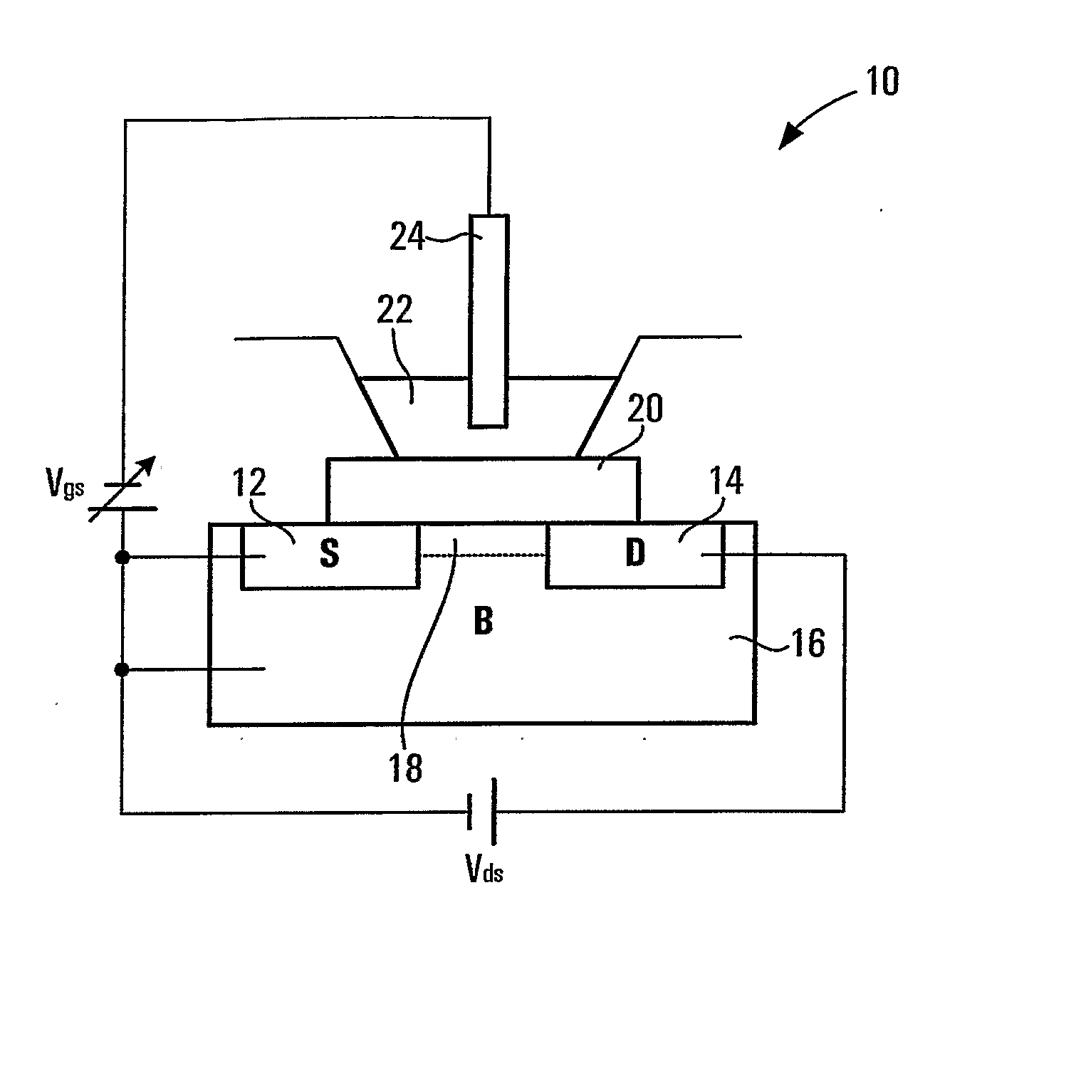
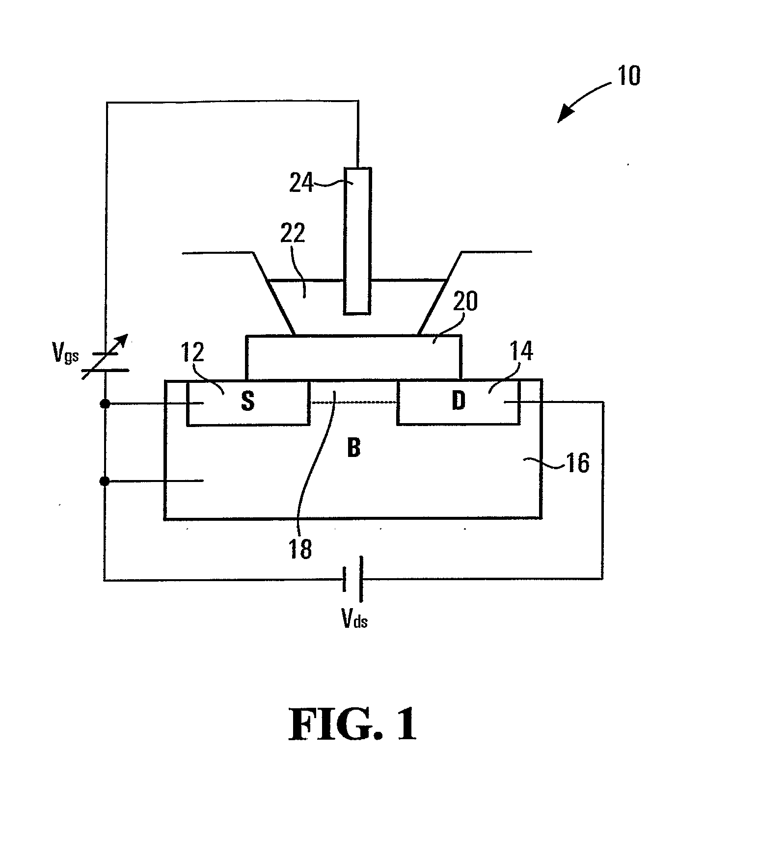
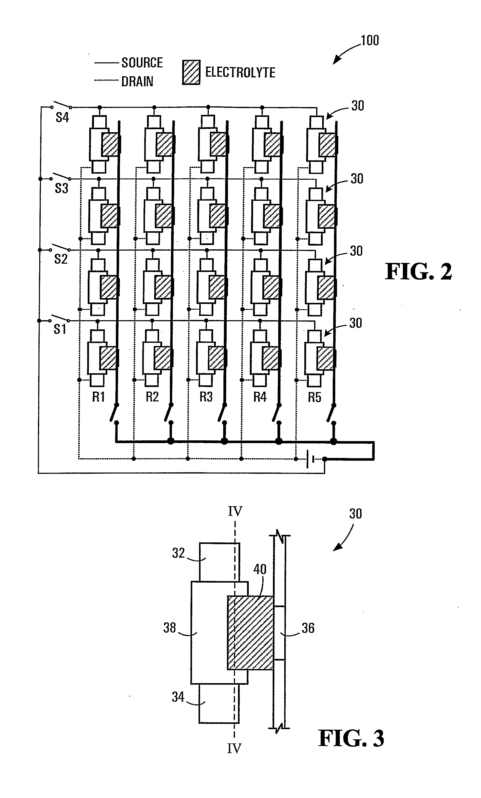
[0030] The invention provides a chemically modified organic field effect transistor (CHEMOFET) based and column-and-row addressable array biochip. Embodiments utilize all printed OFETS in both the sensing and detecting components, combining molecular electronics (building a detection circuit with OFET) and bioelectronics (building an electronic biochip with OFET) to allow the manufacture of a high density array.

[0031] An example single OFET 10 that may be used as a sensor is illustrated in FIG. 1. As illustrated, source and drain electrodes 12, 14 are formed in a semiconducting substrate 16. A channel 18 is formed between source and drain electrodes 12, 14. A dielectric insulating layer 20 is formed atop channel 18. Layer 20 is coated with an electrolyte 22. A reference electrode 24 contacts electrolyte 22 as a substitute for a conventional gate electrode. Probe molecules (not shown) are immobilized in dielectric layer 20 or in electrolyte 22 on top of the dielectric layer 20. Prob...


PUM


Abstract

A bioelectronic microchip formed on a substrate (16) includes a plurality of field effect transistors (10), each including first (12) and second (14) electrodes on the substrate; and a channel (18) extending between the first and second electrodes. An organic semiconducting material fills the channel (18); and a dielectric layer (20) formed atop the first and second electrodes and the channel. An electrolyte (22) to hold a probe molecule may be formed on the dielectric. A third electrode (24) in proximity with the first and second electrodes and isolated therefrom contacts the dielectric. Capture of target molecules may be detected at each transistor through changes in source to drain characteristics. The method provides high density and low cost sensors, particularly in diagonistic and drug discovery applications.

Description

CROSS-REFERENCE TO RELATED APPLICATIONS [0001] This application claims benefits from U.S. Provisional Patent Application No. 60 / 558,117 filed Apr. 1, 2004, the contents of which are hereby incorporated herein by reference.FIELD OF THE INVENTION [0002] The present invention relates generally to addressable biochips, and more particularly to chips incorporating field effect transistors and methods of use thereof. Embodiments of the invention can be used in assays to detect molecular interactions such as nucleic acid hybridization, protein binding or other chemical / electrochemical reactions. BACKGROUND OF THE INVENTION [0003] Chemically modified field effect transistor (CHEMFET)-based sensor technologies have been studied as they have potential as microsensors for food, biomedical and environmental analytics. CHEMFETs have advantages over conventional ion-selective electrode-based sensors in terms of small dimensions, low-output impedance, fast response, mass-fabrication ability and gr...

Claims


Application Information

Patent Timeline
IPC IPC(8): H01L27/28H01L51/40G01N27/403G01N27/414G01N27/416H01L27/088
CPCG01N27/4145
Inventor LI, CHANGMINGSUN, CHANG QING
Owner NANYANG TECH UNIV
Why Eureka
Try Eureka