Surface Inspection Method and Surface Inspection Apparatus

a surface inspection and surface technology, applied in the direction of material analysis, semiconductor/solid-state device testing/measurement, instruments, etc., can solve the problem of generating a difference in detection sensitivity

Inactive Publication Date: 2008-01-17
HITACHI HIGH-TECH CORP
View PDF13 Cites 30 Cited by
  • Summary
  • Abstract
  • Description
  • Claims
  • Application Information

AI Technical Summary

Benefits of technology

[0023] It is possible to realize a surface inspection method and a surface inspection apparatus capable of inspecting a contaminant particle and a defect, or surface roughness with a uniform sensitivity without depending on a rotation angle in a primary scan direction, even in the case where intensity of scattered light generated derived from a contaminant particle and a defect existing on the surface of a semiconductor wafer or adjacent to the surface, or surface roughness of the semiconductor wafer has anisotropy which depends on an illumination direction.

Problems solved by technology

Furthermore, a crystal defect existing in a shallow region adjacent to the substrate surface and surface roughness of the substrate surface are also become inspection objects other than the contaminant particle and the defect as the inspection of the surface of the semiconductor substrate.
Therefore, it is to be expected that there generates a difference in detection sensitivity and there arises an error when the size of the contaminant particle and the defect are calculated on the basis of the scattered light intensity.

Method used


Image

  • Surface Inspection Method and Surface Inspection Apparatus
  • Surface Inspection Method and Surface Inspection Apparatus
  • Surface Inspection Method and Surface Inspection Apparatus

Examples


first embodiment

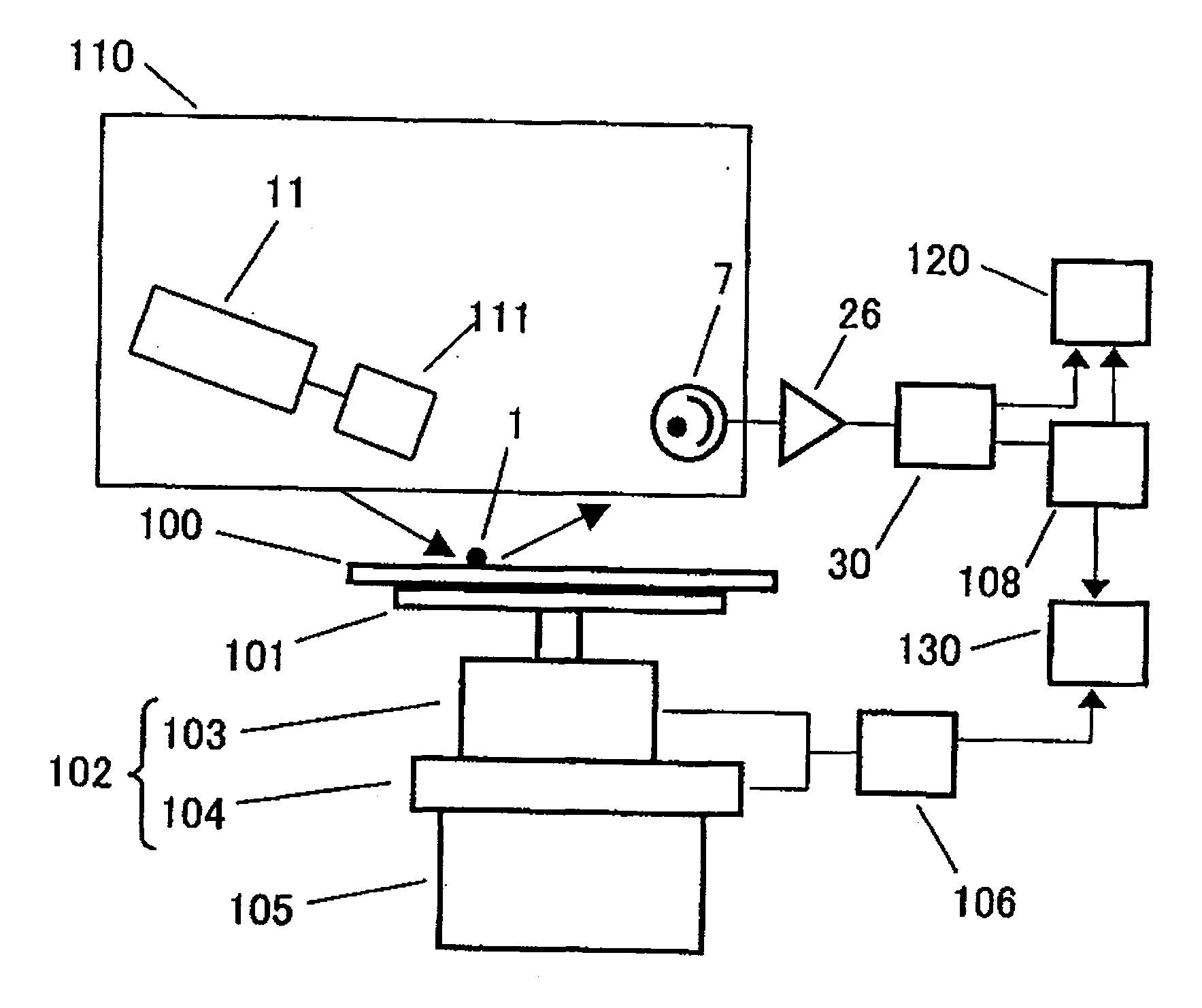
[0042]FIG. 1 is a schematic configuration view of a contaminant particle and defect inspection apparatus according to the present invention. In FIG. 1, a semiconductor wafer 100 that is an object to be inspected is vacuum-contacted to a chuck 101, and the chuck 101 is mounted on a movement stage for an object to be inspected 102 provided with a rotation stage 103 and a translation stage 104, and a Z stage 105.

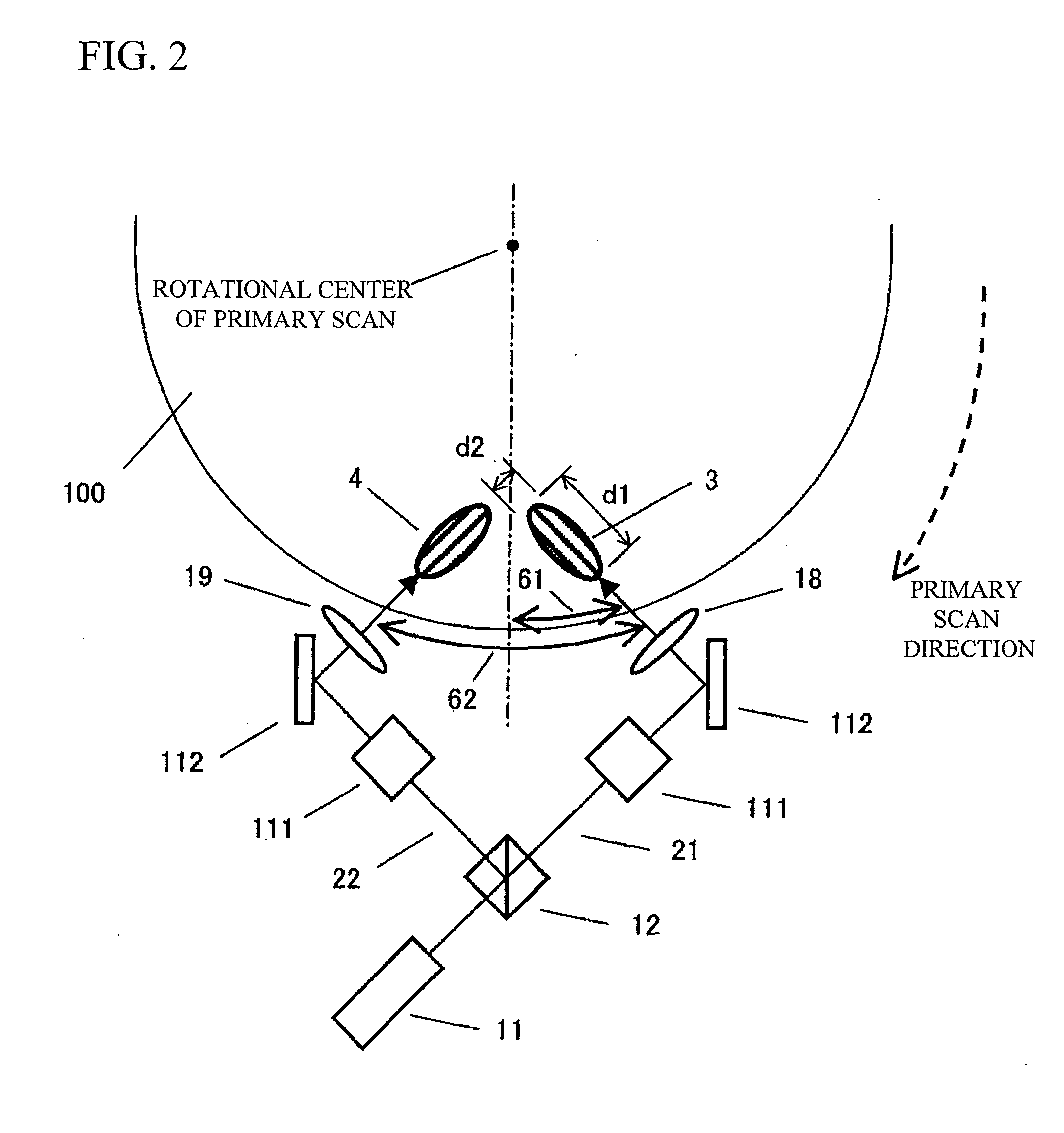
[0043] Illumination and detection optics 110 arranged above the semiconductor wafer 100 are optics shown in FIG. 2 and FIG. 3. FIG. 2 is a plan view of the optics, and FIG. 3 is a side view of the optics.

[0044] In FIG. 2 and FIG. 3, a light source 11 of illumination light in the illumination and detection optics 110 uses a pulse laser which performs pulse oscillation by time repeating light of a wavelength in a UV region. The light outputted from the light source 11 is divided into two illumination beams 21 and 22 by a beam splitter 12.

[0045] The illumination beam 21 reaches ...

second embodiment

[0070]FIG. 5 and FIG. 6 are explanation views of detection optics of the present invention, and showing an example which detect scattered, diffracted, and reflected lights from a plurality of azimuth directions by arranging detection optics in a plurality of directions in which a plurality of elevation angles and a plurality of azimuthal angles are combined. In addition, FIG. 5 is a plan view of the detection optics; and FIG. 6 is a side view of the detection optics.

[0071] Illumination optics in the second embodiment of the present invention is equivalent to the first embodiment, and therefore their explanation will not be described herein.

[0072] A detection system of scattered, diffracted, and reflected lights in the second embodiment of the present invention includes a first elevation angle detection system 70 including four condenser elements 71 which have first substantially equal elevation angles, differ each other with respect to a primary scan rotation axis of a movement sta...

third embodiment

[0086] In the present invention, time instant and interval of time at which illumination light are actually irradiated to the respective illumination spots 3 and 4 can be exactly known by the former light emitting timing signal generating units (14, 15, 16, and 17). Consequently, if an output signal shown in FIG. 11(E) from the photodetector 7 is separated using the light emitting timing signal, it is possible to separate the scattered, diffracted, and reflected light signals from a plurality of the illumination spots 3 and 4 and to detect using one photodetector 7 only.

[0087] More specifically, an output signal of the photodetector 7 is processed by a separation circuit having a configuration shown in FIG. 13. That is, the output signal of the photodetector 7 is amplified by a preamplifier 25, and then, distributed into two gate circuits 27a and 27b. ON and OFF operations of the respective gate circuits 27a and 27b are controlled in accordance with the light emitting timing signals...


PUM

PropertyMeasurementUnit
angleaaaaaaaaaa
azimuthal anglesaaaaaaaaaa
Brewster's angleaaaaaaaaaa

Abstract

In order to realize a surface inspection apparatus capable of inspecting a contaminant particle and a defect with a uniform sensitivity without depending on a rotation angle in a primary scan direction even in the case where intensity of scattered light, which is generated derived from the contaminant particle and the defect existing on the surface of a semiconductor wafer or adjacent to the surface, has anisotropy which depends on an illumination direction; light from a light source 11 becomes two illumination beams 21 and 22 by a beam splitter 12, the beams being irradiated onto a semiconductor wafer 100 from two mutually substantially orthogonal azimuthal angles having substantially equal elevation angles to form illumination spots 3 and 4. When the sum of scattered, diffracted, and reflected lights due to the illumination beams 21 and 22 is detected; influence of the anisotropy which a contaminant particle and a defect existing in the wafer 100 itself or thereon have with respect to an illumination direction, can be eliminated. This makes it possible to inspect a contaminant particle, defect, and the like with a uniform sensitivity without depending on a rotation angle in a primary scan direction even in the case where intensity of the scattered light generated derived from the contaminant particle, defect, and the like depends on the illumination direction.

Description

BACKGROUND OF THE INVENTION [0001] 1. Field of the Invention [0002] The present invention relates to a surface inspection method which measures information on a minute contaminant particle and a defect on a semiconductor substrate (semiconductor wafer), and surface roughness of the substrate. [0003] 2. Description of the Related Art [0004] In a production line for semiconductor substrates (semiconductor wafers), inspection for defects such as a contaminant particle attached to the surface of the semiconductor substrate and a scratch generated during processing is performed in order to observe a state where dust is generated in a manufacturing apparatus. For example, in the semiconductor substrate before forming a circuit pattern, a minute contaminant particle and a defect not larger than several 10 nm on the surface thereof need to be detected. Furthermore, a crystal defect existing in a shallow region adjacent to the substrate surface and surface roughness of the substrate surface ...

Claims


Application Information

Patent Timeline
Patent Type & Authority Applications(United States)
IPC IPC(8): G01N21/88
CPCG01N21/9501H01L22/12H01L2924/0002H01L2924/00
Inventor MATSUI, SHIGERUHACHIYA, MASAYUKI
Owner HITACHI HIGH-TECH CORP
Why Eureka
Try Eureka