High-speed signal transmission structure having parallel disposed and serially connected vias

a signal transmission and high-speed technology, applied in the direction of printed circuit aspects, printed circuit adaptations, printed circuit manufacturing, etc., can solve the problems of unsatisfactory degrade signal integrity, requiring drilling equipment, and misalignment to the multiple layers of the circuit board, so as to prevent the resonance effect and ensure the integrity

Active Publication Date: 2008-01-24
INVENTEC CORP
View PDF0 Cites 9 Cited by
  • Summary
  • Abstract
  • Description
  • Claims
  • Application Information

AI Technical Summary

Benefits of technology

[0009]It is therefore an objective of this invention to provide a high-speed signal transmission structure having parallel-disposed and serially-connected vias that allow a reduction in the resonance effect caused by open stubs without having to employ the back-drill method.
[0011]The high-speed signal transmission structure according to the invention is designed for use on a multi-layer circuit board, such as a high-speed digital circuit board, for providing a signal transmission path through electrically-conductive vias that can help prevent resonance effect in the high-speed signal transmitting therethrough to thereby ensure the signal integrity.
[0012]The high-speed signal transmission structure according to the invention is characterized by the provision of a pair of parallel-disposed and serially-connected vias extending between the upper layer and the bottom layer of the multi-layer circuit board for interconnecting two signal lines on different layers of the circuit board, for the purpose of shorting the open stub in the signal transmission line to help prevent resonance effect and thereby ensure the integrity of the high-speed signal being transmitted therethrough.

Problems solved by technology

The existence of the open stub 132 would then undesirably cause the transmitting high-speed signal to be subject to resonance and thus undesirably degrade signal integrity.
In practice, however, this method has several drawbacks, such as requiring the use of drilling equipment which is costly and time-consuming to implement, and would easily cause misalignment to the multiple layers of the circuit board 10.

Method used


Image

  • High-speed signal transmission structure having parallel disposed and serially connected vias
  • High-speed signal transmission structure having parallel disposed and serially connected vias
  • High-speed signal transmission structure having parallel disposed and serially connected vias

Examples


Embodiment Construction

[0018]The high-speed signal transmission structure according to the invention is disclosed in full details by way of preferred embodiments in the following with reference to the accompanying drawings.

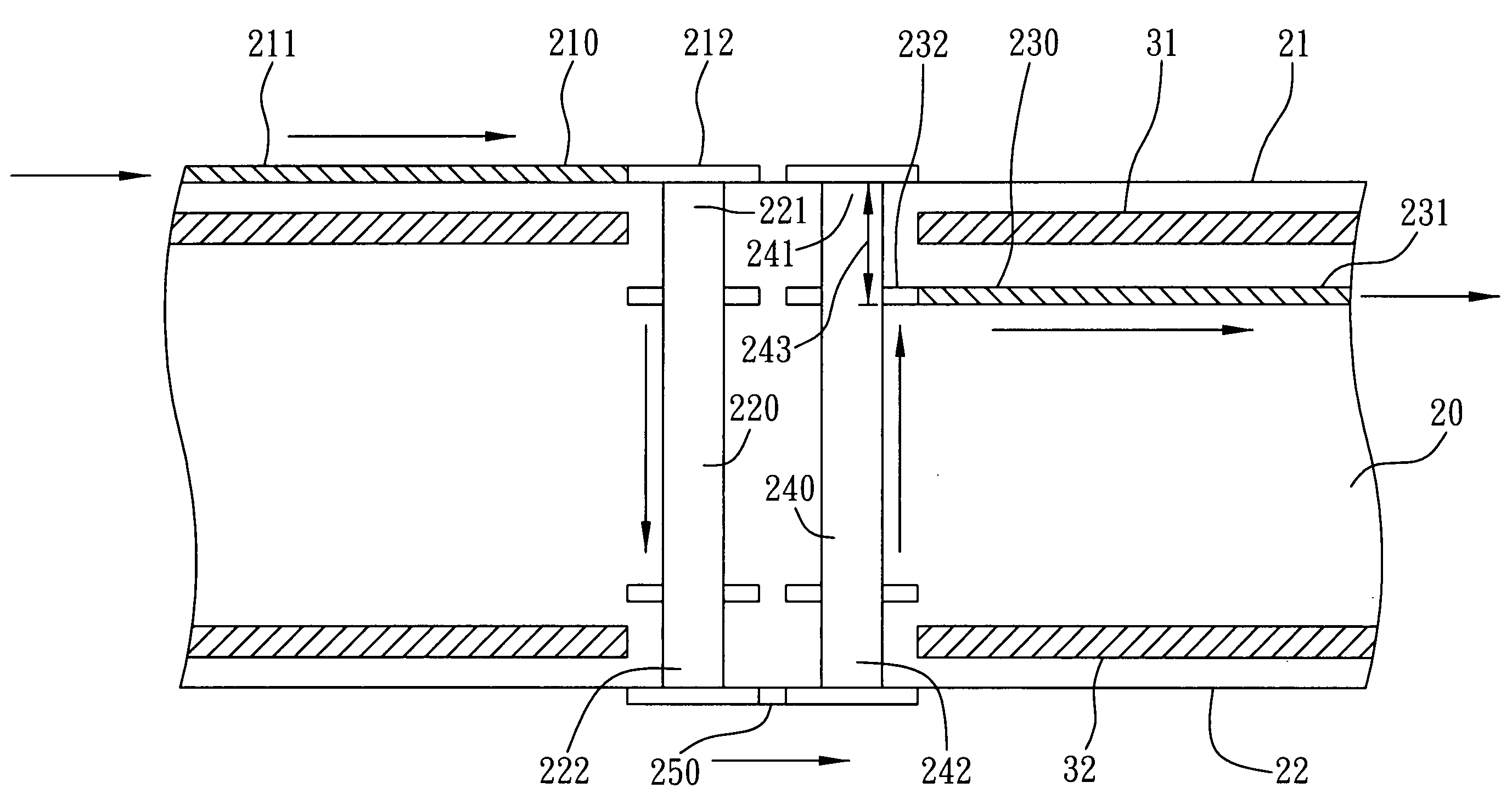
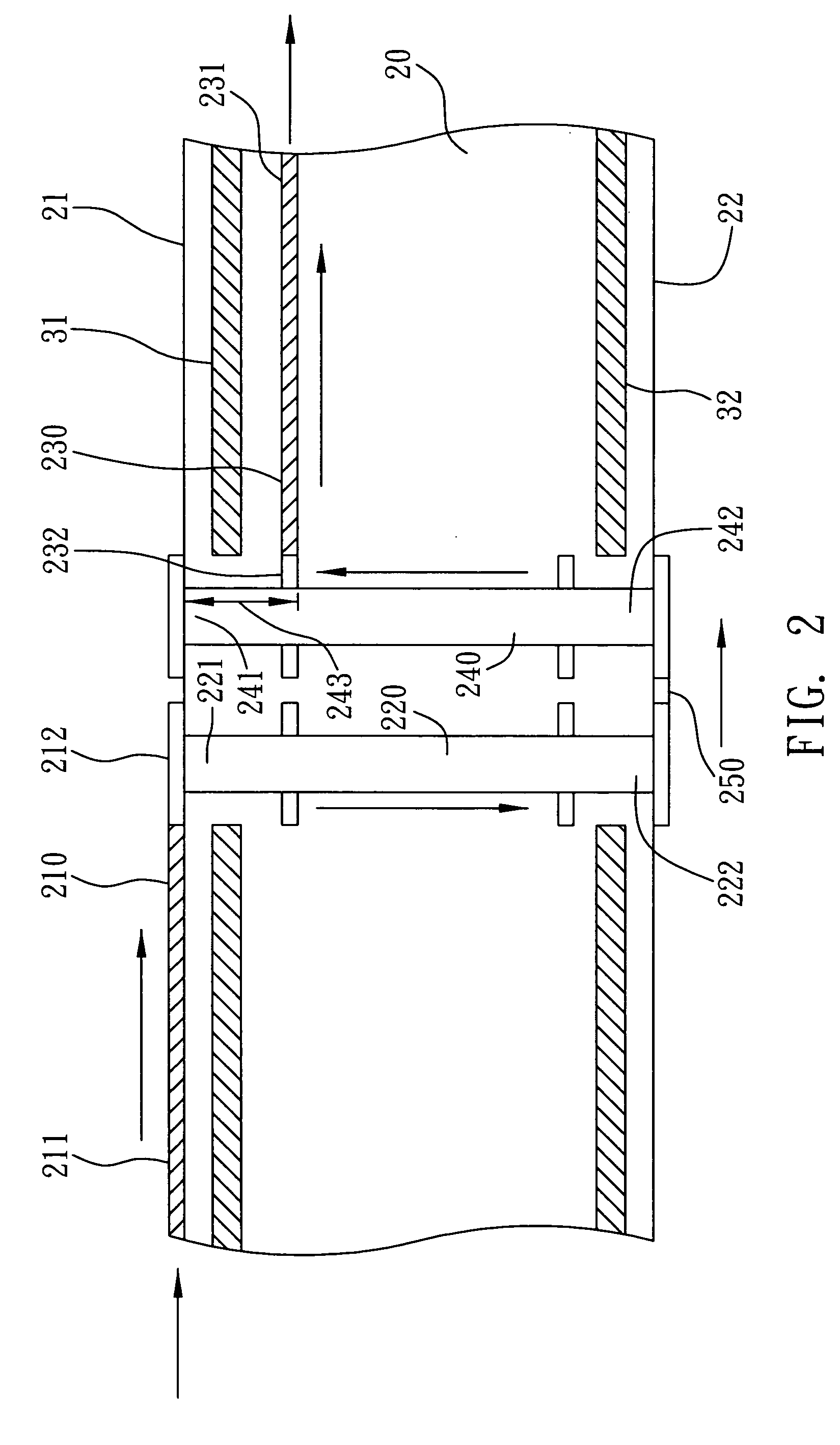
[0019]FIG. 2 show the application of the high-speed signal transmission structure of the invention. As shown, the high-speed signal transmission structure of the invention is designed for use on a multi-layer circuit board 20, such as a high-speed digital circuit board for wireless networking, mobile phone, GPS, or digital TV, to name just a few, where the multi-layer circuit board 20 is constructed on a multi-layer structure of the type having at least one upper layer 21 and one bottom layer 22 with at least one upper reference plane 31 formed on the internal side of the upper layer 21 and one bottom reference plane 32 formed on the internal side of the bottom layer 22 (it is to be noted that FIG. 2 only demonstratively shows two layers 21, 22 in the multi-layer circuit board 20; in pr...


PUM


Abstract

A high-speed signal transmission structure having parallel disposed and serially connected vias is disclosed. The structure is applicable to a multi-layered circuit board such as a high-speed digital circuit board for forming a high-speed signal transmission circuit on the high-speed digital circuit board. The structure includes a pair of parallel disposed and serially connected vias for connecting an upper conductive circuit installed on an upper layer of the multi-layered circuit board and a lower conductive circuit installed on a lower layer of the multi-layered circuit board. Compared with the prior art, an open stub formed by the remaining portion of the vias has become shorter, thereby reducing a resonance effect affecting the quality of signal transmission.

Description

BACKGROUND OF THE INVENTION[0001]1. Field of the Invention:[0002]This invention relates to high-speed digital circuit technology, and more particularly, to a high-speed signal transmission structure having parallel-disposed and serially-connected vias which is designed for use on a multi-layer circuit board, such as a high-speed digital circuit board, for providing a signal transmission path through the signal electrically-conductive vias that can help prevent resonance effect in the high-speed signal transmitting therethrough to thereby ensure the signal integrity of the transmitted signal.[0003]2. Description of Related Art:[0004]With the advent of wireless digital communication technologies, such as wireless networking, mobile phones, GPS (Global Positioning System), etc., the design and manufacture of high-speed digital circuit boards that handle digital signals within the gigahertz range is in high demand in the electronics industry. In circuit layout design, high-speed digital...

Claims


Application Information

Patent Timeline
Patent Type & Authority Applications(United States)
IPC IPC(8): H05K1/11H01R12/04
CPCH05K1/0251H05K2201/09627H05K3/429H05K1/115
Inventor CHEN, YEN-HAO
Owner INVENTEC CORP
Why Eureka
Try Eureka