Organic Electroluminescent Device and Manufacturing Method Thereof

a technology of electroluminescent devices and manufacturing methods, which is applied in the manufacture of electric discharge tubes/lamps, instruments, and discharge tubes luminescent screens. it can solve the problems of difficult photolithography, blunt pattern, and basic problems of photolithography, and achieve high-precision luminescent pattern patterns and good display quality.

Inactive Publication Date: 2008-01-24
TORAY IND INC
View PDF3 Cites 167 Cited by
  • Summary
  • Abstract
  • Description
  • Claims
  • Application Information

AI Technical Summary

Benefits of technology

[0020] This invention can provide an organic electroluminescent device with good display quality, in which a highly precise pattern of a luminescent layer can be formed in the entire area.

Problems solved by technology

For forming the first electrodes of the organic electroluminescent device, photolithography can be applied, but for forming the luminescent layer and the second electrodes, it is often difficult to apply photolithography, since photolithography basically has problems owing to a wet process.
Further, if the mask member is thick, shadowing due to the deposition angle occurs and makes the pattern blunt.
This mask has a problem that an in-plane stress difference occurs between the mask area and the opening area depending on mask manufacturing conditions, and that local bending occurs at the boundary portion {the dotted line portion of FIG. 3 (a)}.
Especially in the case where the pitch of pixel sets, each set consisting of one each luminescent pixel of respective colors, is 500 μm or less, the colors of adjacent luminescent pixels are likely to be mixed, not allowing fine light emission to be obtained.
This problem is more likely to occur for exerting larger influence when the boundaries are straight and longer, because of the nature of bending at the boundary portion between the mask area and the opening area.
That is, this problem is more outstanding when the screen is larger-sized with longer sides.
However, these techniques are not able to inhibit local bending.
Further, as the deposition mask for forming the second electrodes in conformity with a predetermined pattern, disclosed is a means for lessening the applied tension by dividing the mask member (for example, see Patent Document 2), but this technique is considered to be insufficient for higher precise patterning of the luminescent layer.
Further, as a multiple luminescent area deposition mask, it is also known that if the mask member is stuck to a frame with n openings, productivity can be enhanced (for example, see Patent Document 3), but this technique is not effective for inhibiting the local bending of the mask member.
Moreover, since it is necessary to align the two mask members, i.e., the striped first mask member and the second mask member to the object for deposition, the technique is disadvantageous in view of productivity.
Furthermore, the second mask member may cause shadowing and raise the risk of producing defective products.

Method used


Image

  • Organic Electroluminescent Device and Manufacturing Method Thereof
  • Organic Electroluminescent Device and Manufacturing Method Thereof
  • Organic Electroluminescent Device and Manufacturing Method Thereof

Examples


example 1

[0085] A 1.1 mm thick alkali-free glass substrate with a 130 nm thick ITO (indium tin oxide) transparent electrode film formed by sputtering on the surface of the glass substrate was cut to a size of 120×100 mm. The ITO substrate was coated with a photoresist, and the laminate was exposed and developed for patterning by ordinary photolithography. The unnecessary portions of ITO were removed by etching, and subsequently the photoresist was removed to form 90 mm long and 80 μm wide stripes from the ITO film in conformity with a predetermined pattern. The stripes were 816 first electrodes disposed at a pitch of 100 μm.

[0086] Then, a positive photoresist (OFPR-800 produced by Tokyo Ohka Kogyo Co., Ltd.) was applied to have a thickness of 3 μm by spin coating on the substrate with the first electrodes formed on it. The coating film formed of the photoresist was exposed pattern-wise through a photo mask and developed to be patterned. The development was followed by curing at 180° C. Thus...

example 2

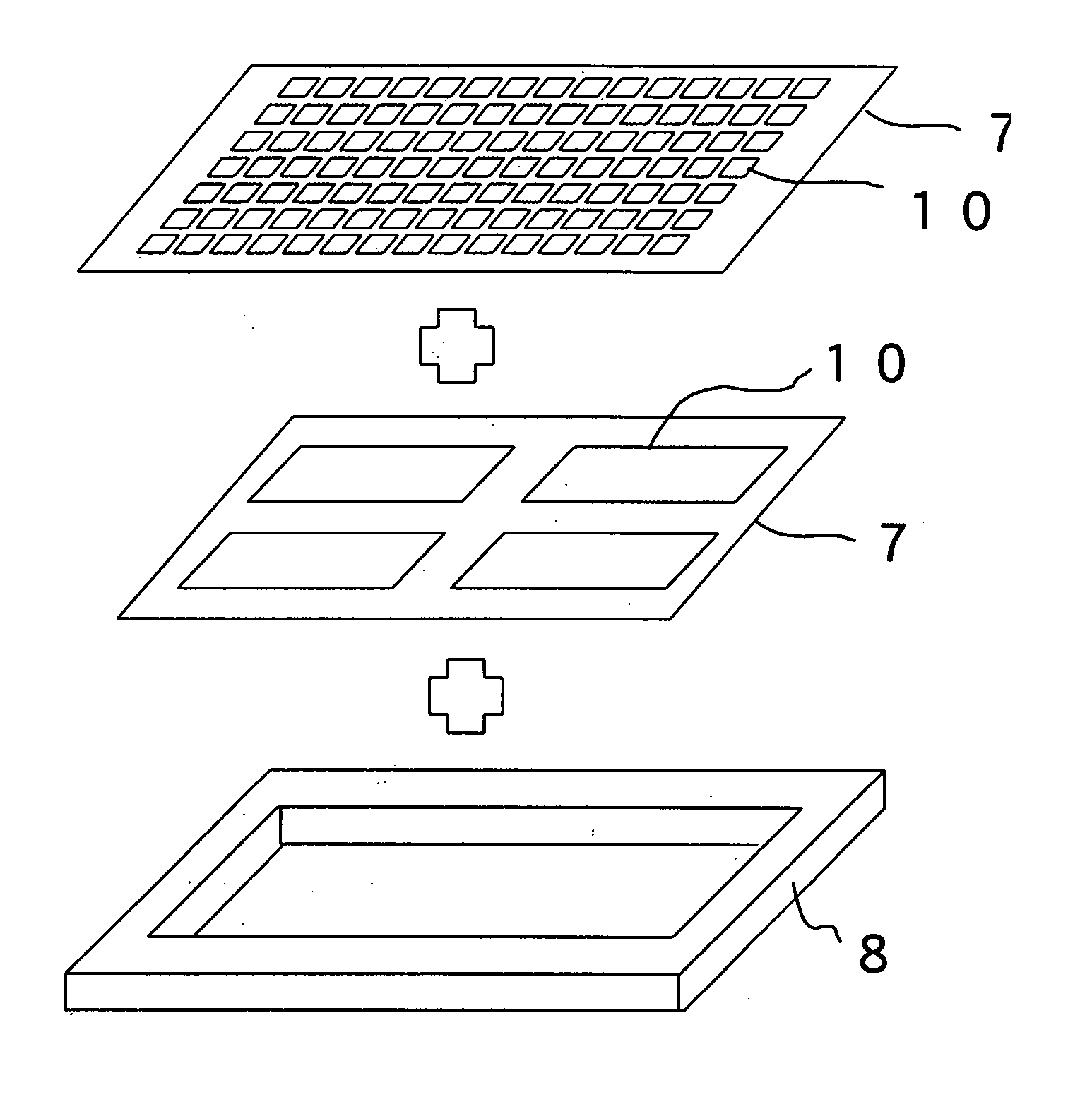
[0099] An organic electroluminescent device was prepared as described in Example 1, except that the deposition mask for the luminescent layer had a effective area consisting of 200 openings in the lengthwise direction and 272 openings in the crosswise direction and that circular dummy openings with a diameter of 200 μm were arranged at a pitch of 400 μm in an area of 3 mm around the effective opening area, as shown in FIG. 10.

[0100] The organic electroluminescent device was driven by line sequential drive, and good display characteristics could be obtained. Further, through a microscope observation to the luminescent pixels, it was confirmed that mixing between adjacent pixels did not occur and that a good luminescent layer pattern could be formed over the entire surface of the luminescent area.

example 3

[0101] A 1.1 mm thick alkali-free glass substrate with a 130 nm thick ITO transparent electrode film formed by sputtering on the surface of the glass substrate was cut to a size of 120×100 mm. The ITO substrate was coated with a photoresist, and the laminate was exposed and developed by ordinary photolithography for patterning. The unnecessary portions of ITO were removed by etching, and subsequently the photoresist was removed to form 90 mm long and 160 μm wide stripes from the ITO film in conformity with a predetermined pattern. Four hundred and eight striped first electrodes were disposed at a pitch of 200 μm.

[0102] Then, a positive photoresist (OFPR-800 produced by Tokyo Ohka Kogyo Co., Ltd.) was applied to have a thickness of 3 μm by spin coating on the substrate having the first electrodes formed on it. The coating film formed of the photoresist was exposed pattern-wise through a photo mask and developed to be patterned. The development was followed by curing at 180° C. Thus,...


PUM

PropertyMeasurementUnit
distanceaaaaaaaaaa
widthaaaaaaaaaa
thicknessaaaaaaaaaa

Abstract

A highly fine organic electroluminescent device is provided. A method for manufacturing the organic electroluminescent device is provided for patterning a very fine light emitting layer, and a deposition mask is provided to be used in the patterning. For deposition of the light emitting layer, a mask member is provided with apertures (effective apertures) for forming the light emitting layer to be used for light emitting pixel and apertures (dummy apertures) not to be used for forming the light emitting pixel around an area (effective aperture area) separated by the outer edge of a group of the apertures. The light emitting layer is deposited by using the deposition mask.

Description

TECHNICAL FIELD [0001] The present invention relates to an organic electroluminescent device including a luminescent layer composed of organic compounds and formed as a pixel pattern by a mask deposition method, and also relates to a manufacturing method thereof. BACKGROUND ART [0002] An organic electroluminescent device emits light when the positive holes injected from an anode and the electrons injected from a cathode are recombined in an organic luminescent layer kept between both the electrodes. As a typical structure of it, as shown in FIG. 2, first electrodes 2 formed on a substrate 1, thin film layers including at least a luminescent layer 5 composed of organic compounds, and second electrodes 6 are formed on it, and the light emitted by such recombination goes out through the transparent electrodes to outside. Such an organic electroluminescent device is thin and-allows high-brightness light emission at a low driving voltage or multi-color light emission by selecting the org...

Claims


Application Information

Patent Timeline
Patent Type & Authority Applications(United States)
IPC IPC(8): H01J1/62H01L27/28H05B33/10
CPCC23C14/042C23C14/12C23C14/26H01L51/56H01L27/3223H01L51/0011G03F1/20H10K59/88H10K71/166H10K71/00
Inventor ARAI, TAKESHIFUJIMORI, SHIGEOIKEDA, TAKESHI
Owner TORAY IND INC
Why Eureka
Try Eureka