
Display Device and Fabrication Method Thereof

Inactive Publication Date: 2008-01-31
HITACHI DISPLAYS
View PDF1 Cites 4 Cited by
  • Summary
  • Abstract
  • Description
  • Claims
  • Application Information

AI Technical Summary

Benefits of technology

[0006]However, in the above-mentioned method which uses the continuous oscillation laser, a melting time of silicon is long and hence, due to a surface tension of molten silicon, silicon is aggregated at the frequency of approximately 1.4 pieces / cm2 empirically. When such aggregation occurs, portions where a silicon layer is not formed are present on the insulation substrate and hence, the thin film transistor becomes inoperable thus giving rise to lowering of a fabrication yield rate.
[0008]However, it is necessary for the silicon oxide film which constitutes the background to ensure a certain film thickness and hence, the use of only one of the silicon oxide film A and the silicon oxide film B is difficult to obtain the thin film transistor having desired properties while suppressing aggregation. Here, as a method for suppressing the generation of aggregation of a molten silicon film by reducing the influence of a surface tension by enhancing the wettability of the silicon film with a background film (silicon oxide film), a method which uses a film exhibiting small polarizability to a silicon oxide film as a background film is disclosed in patent document 1.
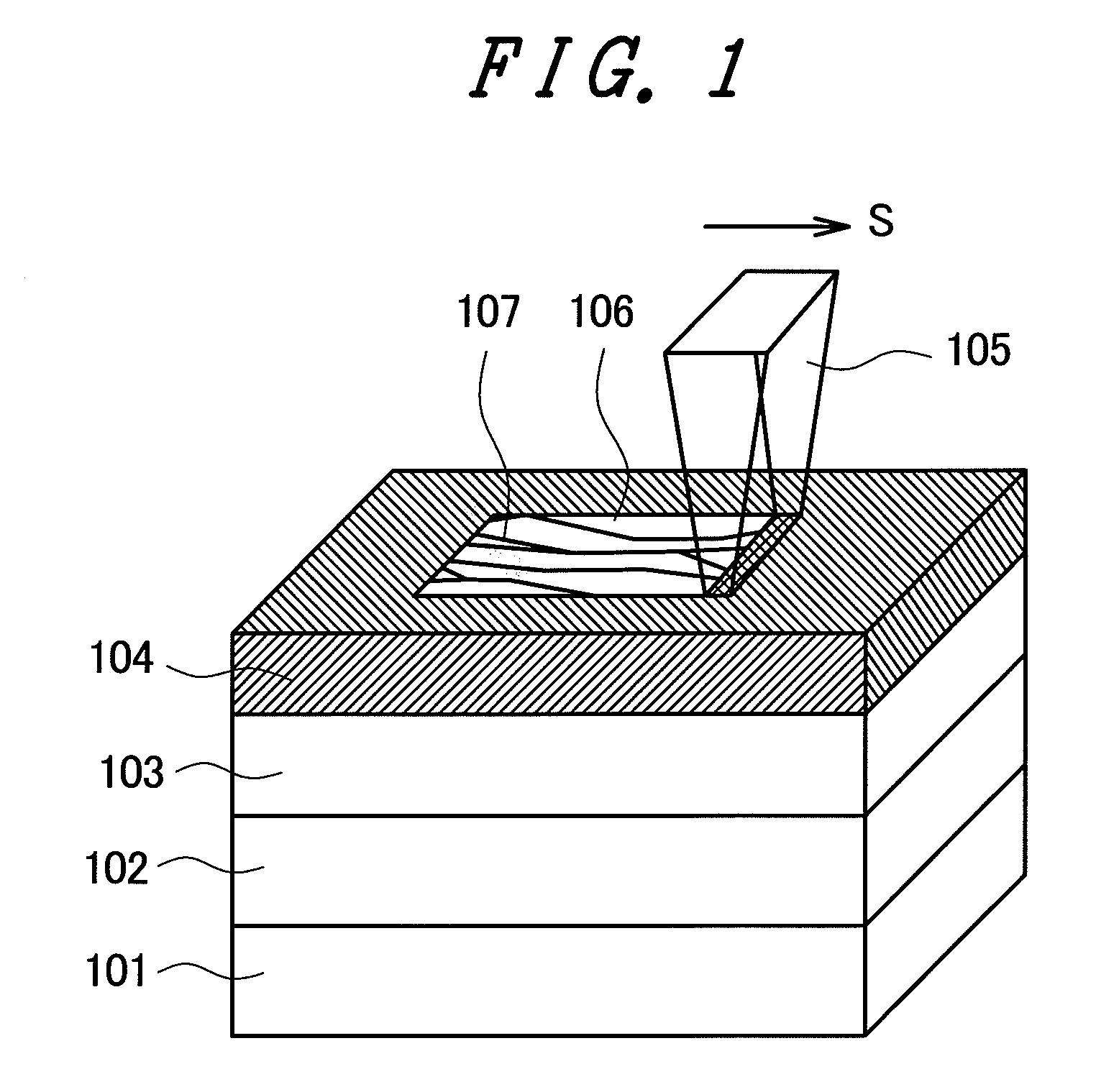
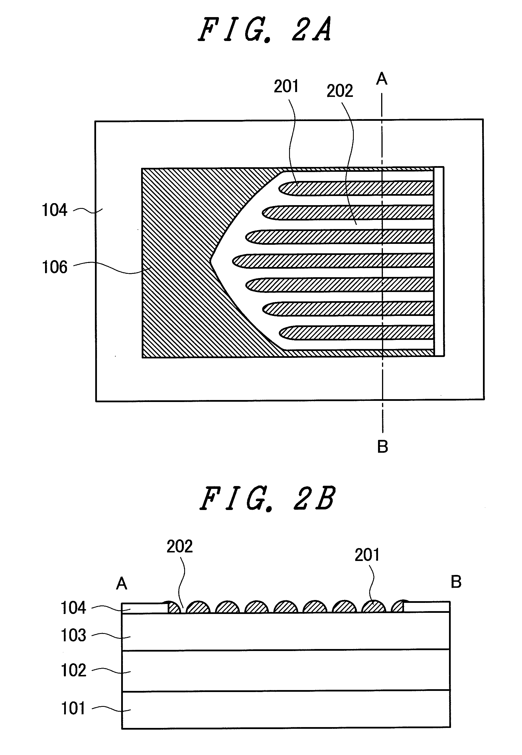
[0009]It is an object of the present invention to provide a system-in-panel display device which uses a high functional thin film transistor by suppressing aggregation of a molten semiconductor at the time of allowing strip-like pseudo-single crystals to continuously grow with a directional control by radiating beams to a semiconductor film made of silicon or the like using a continuous oscillation laser while scanning.
[0015]By forming the silicon oxide film into the two-layered structure constituted of the silicon oxide film A and the silicon oxide film B without changing a total film thickness of the silicon oxide film, aggregation yield rate and the transistor characteristic can be controlled to obtain desired aggregation yield rate and a transistor characteristic thus achieving both suppression of aggregation and enhancement of the transistor characteristic whereby a high-definition system-in panel display device can be realized.

Problems solved by technology

However, in the above-mentioned method which uses the continuous oscillation laser, a melting time of silicon is long and hence, due to a surface tension of molten silicon, silicon is aggregated at the frequency of approximately 1.4 pieces / cm2 empirically.
When such aggregation occurs, portions where a silicon layer is not formed are present on the insulation substrate and hence, the thin film transistor becomes inoperable thus giving rise to lowering of a fabrication yield rate.
However, it is necessary for the silicon oxide film which constitutes the background to ensure a certain film thickness and hence, the use of only one of the silicon oxide film A and the silicon oxide film B is difficult to obtain the thin film transistor having desired properties while suppressing aggregation.

Method used


Image

  • Display Device and Fabrication Method Thereof
  • Display Device and Fabrication Method Thereof
  • Display Device and Fabrication Method Thereof

Examples


embodiment 1

[0028]In an embodiment 1, a following method which is obtained based on an actual experimental result is explained.

[0029](1) When the silicon oxide film is formed of the two-layered structure, the silicon oxide film exhibits an aggregation suppression effect and a transistor characteristic which fall between an aggregation suppression effect and a transistor characteristic when a silicon oxide film A is formed of a single layer and an aggregation suppression effect and a transistor characteristic when a silicon oxide film B is formed of a single layer. Accordingly, by controlling film thicknesses of the silicon oxide film A and the silicon oxide film B, it is possible to control the suppression of aggregation and the transistor characteristic of the silicon oxide film.

[0030](2) The characteristic of the silicon oxide film which is brought into contact with the silicon layer exhibits a larger effect. When the silicon oxide film A and the silicon oxide film B have the same film thickn...


PUM


Abstract

The present invention obtains a system-in-panel display device using a high-performance thin film transistor by suppressing aggregation of a molten semiconductor at the time of allowing strip-like pseudo-single crystal to grow continuously with a direction control by radiating beams of continuous oscillation laser to a semiconductor film made of silicon while scanning. A display device includes a silicon nitride film formed on the insulation substrate, a silicon oxide film formed on the silicon nitride film, a semiconductor film formed on the silicon oxide film, and a thin film transistor which uses the semiconductor film. Here, the silicon oxide film is constituted of a first silicon oxide film formed using SiH4 and N2O as raw material gases and a second silicon oxide film formed using a TEOS gas as a raw material gas, and the semiconductor film is made of pseudo-single crystal having strip-like grains.

Description

[0001]The present application claims priority from Japanese applications JP2006-202712 filed on Jul. 26, 2006, the content of which is hereby incorporated by reference into this application.BACKGROUND OF THE INVENTION[0002]The present invention relates to a display device and a fabrication method thereof, and more particularly to a display device and a fabrication method which are suitable for the manufacture of an active-matrix flat-panel display device.[0003]In an active-matrix flat-panel display device such as a liquid crystal display device or an organic EL display device, on a main surface of an insulation substrate made of glass or the like which arranges pixels two-dimensionally in a matrix array, a drive circuit which uses thin film transistors (TFT) for turning on and off the pixels and an auxiliary circuit are mounted thus realizing a high-definition and a high-speed display.[0004]In fabricating a system-in panel which mounts a peripheral circuit including a drive circuit ...

Claims


Application Information

Patent Timeline
IPC IPC(8): H01L29/04H01L21/00
CPCH01L21/02532H01L21/02683H01L27/1285H01L29/04H01L27/1248H01L21/02691
Inventor NODA, TAKESHIKAMO, TAKAHIROOUE, EIJIHATANO, MUTSUKOSATO, TAKESHI
Owner HITACHI DISPLAYS
Learn More