Use of carbon co-implantation with millisecond anneal to produce ultra-shallow junctions

a technology of carbon co-implantation and millisecond annealing, which is applied in the direction of semiconductor devices, electrical apparatus, transistors, etc., can solve the problems of less effective conventional doping by implantation followed by thermal post-annealing, failure of devices, and difficulty in producing ultra-shallow source/drain junctions, etc., and achieves short time thermal annealing

Inactive Publication Date: 2008-01-31
APPLIED MATERIALS INC
View PDF5 Cites 37 Cited by
  • Summary
  • Abstract
  • Description
  • Claims
  • Application Information

AI Technical Summary

Benefits of technology

[0008] The present invention as recited in the claims relates to a method of forming an ultrashallow junction in a substrate. In one embodiment, the method includes providing a silicon substrate, co-implanting the silicon substrate with carbon and a dopant to form a doped silicon substrate, and exposing the silicon substrate to a short time thermal anneal. In certain embodiments, the silicon substrate is exposed to a rapid thermal anneal after co-implanting the silicon substrate but prior to exposing the silicon substrate to a short time thermal anneal. In certain embodiments, a pre-amorphization implant is performed on the silicon substrate prior to implanting the silicon substrate with carbon and a dopant. In certain embodiments, the silicon substrate is a monocrystalline silicon substrate.
[0009] In another embodiment a method of forming an ultra-shallow junction in a substrate is provided. The method includes providing a substrate comprising silicon with a gate dielectric and a gate electrode disposed thereon, performing a pre-amorphization implant of the substrate, co-implanting the substrate with carbon and a dopant to form a source region and a drain region on the substrate, exposing the substrate to a rapid thermal anneal, and exposing the substrate to a short time thermal anneal. In certain embodiments, an ultra-shallow junction is formed between the source region and the drain region having a junction depth less than 21 nm and an abruptness of ≦3 nm / decade.

Problems solved by technology

Such ultra shallow source / drain junctions are becoming more challenging to produce as junction depth is required to be less than 30 nm for sub-100 nm CMOS devices.
Conventional doping by implantation followed by thermal post-annealing is less effective as the junction depth approaches the size of 10 nm, since thermal post-annealing can cause enhanced dopant diffusion.
Dopant diffusion may contaminate nearby layers and cause failure of the device.

Method used


Image

  • Use of carbon co-implantation with millisecond anneal to produce ultra-shallow junctions
  • Use of carbon co-implantation with millisecond anneal to produce ultra-shallow junctions
  • Use of carbon co-implantation with millisecond anneal to produce ultra-shallow junctions

Examples


examples

[0034] The following non-limiting examples are provided to further illustrate embodiments of the invention. However, the examples are not intended to be all-inclusive and are not intended to limit the scope of the inventions described herein.

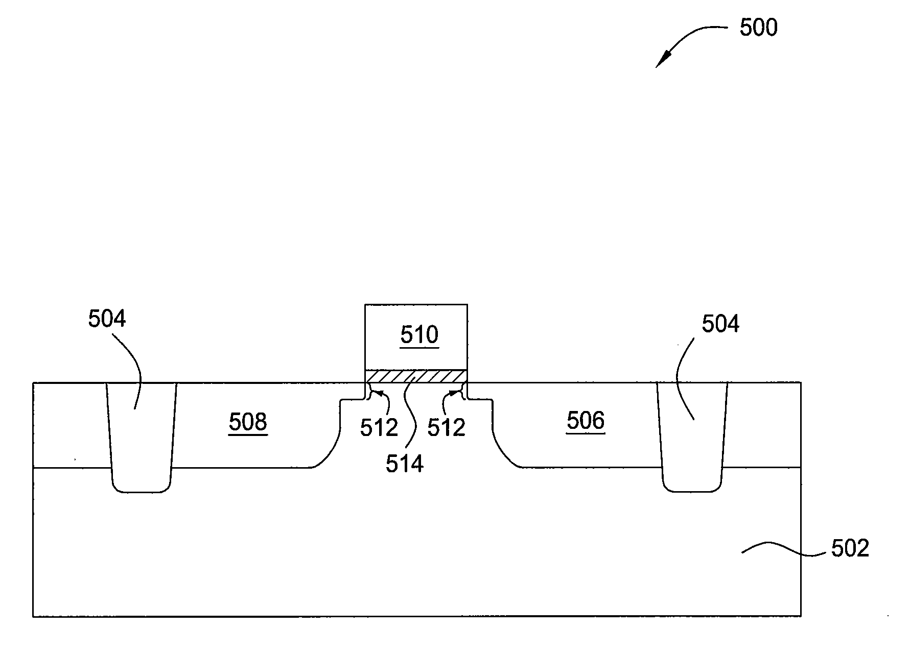
[0035] Blanket wafer and device experiments were carried out on 200 mm Si wafers. To form the ultra-shallow source / drain extension (SDE) with co-implants, a first step of Si or Ge PAI was used. This was followed by a C or F implant and finally a dopant implant. The dopant implants were B for PMOS extensions and P for NMOS extensions. On the device wafers, these extensions were implemented in a conventional transistor flow, primarily with polysilicon gates on SiON gate dielectric but with Ni Fully Silicided (FUSI) gates in some cases.

[0036] Dopant activation and damage annealing was done by a 1050° C. spike anneal unless noted otherwise, and often followed by a sub-melt laser anneal. The implants were carried out on an Applied Materials Quantum...


PUM

PropertyMeasurementUnit
junction depthaaaaaaaaaa
depthaaaaaaaaaa
diameteraaaaaaaaaa

Abstract

Embodiments of the present invention include methods for forming an ultra-shallow junction in a substrate. In one embodiment, the method includes providing a silicon substrate, co-implanting the silicon substrate with carbon and a dopant to form a doped silicon substrate, and exposing the silicon substrate to a short time thermal anneal. In certain embodiments, the silicon substrate is exposed to a rapid thermal anneal after co-implanting the silicon substrate but prior to exposing the silicon substrate to a short time thermal anneal. In certain embodiments, the pre-amorphization implant is performed on the silicon substrate prior to implanting the silicon substrate with carbon and a dopant. In certain embodiments, the silicon substrate is a monocrystalline silicon substrate.

Description

CROSS-REFERENCE TO RELATED APPLICATIONS [0001] This application claims benefit of U.S. Provisional Patent Application No. 60 / 820,750, filed Jul. 28, 2006, which is herein incorporated by reference.BACKGROUND OF THE INVENTION [0002] 1. Field of the Invention [0003] Embodiments of the invention generally relate to the field of semiconductor manufacturing processes, and more particularly, to methods of forming ultrashallow junctions having reduced junction depths and improved dopant activation and profile abruptness. [0004] 2. Description of the Related Art [0005] Integrated circuits may include more than one million micro-electronic field effect transistors (e.g., complementary metal-oxide-semiconductor (CMOS) field effect transistors) that are formed on a substrate (e.g., semiconductor wafer). A CMOS transistor includes a gate structure that is disposed between a source region and a drain region defined in the semiconductor substrate. The gate structure generally comprises a gate ele...

Claims


Application Information

Patent Timeline
Patent Type & Authority Applications(United States)
IPC IPC(8): H01L29/94H01L21/425
CPCH01L21/26506H01L21/26513H01L29/7833H01L29/6659H01L21/324H01L21/2658
Inventor FELCH, SUSAN B.HIGASHI, GREGG S.
Owner APPLIED MATERIALS INC
Why Eureka
Try Eureka