Semiconductor integrated circuit

a technology of integrated circuits and semiconductors, applied in the direction of digital storage, pulse automatic control, instruments, etc., can solve the problems of affecting the operation stability of the integrated circuit, the difficulty of controlling the characteristic variation, and the occurrence of setup errors, so as to reduce power consumption, avoid the effect of holding errors and improved operational stability

Active Publication Date: 2008-01-31
PANASONIC CORP
View PDF7 Cites 6 Cited by
  • Summary
  • Abstract
  • Description
  • Claims
  • Application Information

AI Technical Summary

Benefits of technology

[0029](xii) In the above-mentioned configuration, there is an embodiment that a stop signal generation circuit for controlling the control circuit so that an earth potential is applied to a power supply voltage of aforementioned combinational circuit and a power supply voltage of aforementioned clock buffer when the combinational circuit and the clock buffer get into stop operation, is further provided. Herewith, it is possible to reduce the power consumption in the state where operation is stopped.
[0030]As mentioned above, according to the present invention, the local variation and the like of delay time due to the random variation of the semiconductor integrated circuit consisting of MOSFET etc. can be prevented through controlling the delay time of the flip-flop circuit and the delay time of the combinational circuit independently. Herewith, the operational stability of the semiconductor integrated circuit is improved. More specifically, it is possible to avoid the holding error by adjusting the delay time of the flip-flop circuit. Moreover, it is also possible to avoid the setup error by adjusting the delay time of the combinational circuit.
[0031]Even when the local variation of the delay time due to the random variation of the semiconductor integrated circuit consisting of MOSFET etc. occurs, the technique of the present invention is useful as the semiconductor integrated circuit since it is possible to perform the stable operation by avoiding the holding error and the setup error.

Problems solved by technology

However, in the semiconductor manufacturing technique, although the process variation (Hereafter, it is called “random variation”) generated at random between the plural MOSFETs becomes remarkable along with miniaturisation, it is difficult to control the characteristic variation depending on such a random variation according to the above-mentioned conventional technique for controlling the variation.
For example, in the path to decide an operation frequency, a delay time grows due to the random variation, and a setup error is occurred.
Moreover, in the path where the holding restriction of flip-flop is severe, the delay time decreases by the random variation, and a holding error is occurred.
For this case, it is impossible to avoid both errors at the same time according to the above-mentioned conventional technique for controlling the variation.

Method used


Image

  • Semiconductor integrated circuit
  • Semiconductor integrated circuit
  • Semiconductor integrated circuit

Examples


first embodiment

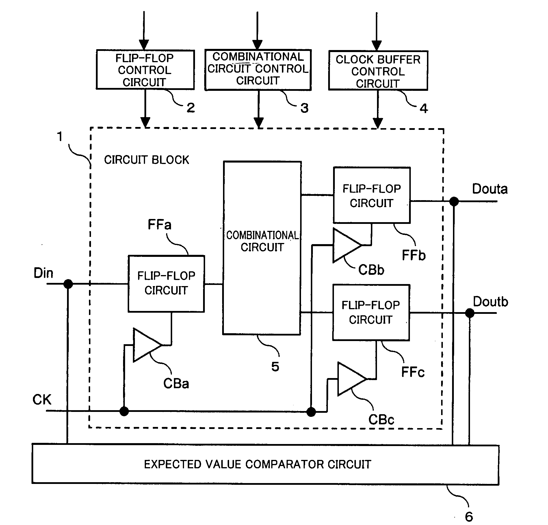
[0045]FIG. 1 is a block diagram showing a configuration of a semiconductor integrated circuit according to the first embodiment of the present invention. As shown in FIG. 1, the semiconductor integrated circuit includes a circuit block 1, a flip-flop control circuit 2, a combinational circuit control circuit 3, a clock buffer control circuit 4, and an expected value comparator circuit 6. The circuit block 1 includes a data input terminal Din, data output terminals Douta and Doutb, a clock input terminal CK, clock buffers CBa, CBb and CBc that distributes a clock, flip-flop circuits FFa, FFb and FFc that are sequential circuits for holding value, and a combinational circuit 5 that is a logic gate such as AND and OR etc. The flip-flop control circuit 2 controls a power supply voltage and a substrate voltage of the flip-flop circuits FFa, FFb and FFc. The combinational circuit control circuit 3 controls the power supply voltage and the substrate voltage of the combinational circuit 5. ...

second embodiment

[0099]Next, in the case where the semiconductor integrated circuit actually operates, described is a second embodiment where the present invention is implemented in a configuration wherein the delay time of the flip-flop circuits FFa, FFb and FFc and the combinational circuit 5 varies due to change of temperature and voltage and degradation in the process etc. As shown in FIG. 6, the semiconductor integrated circuit is equipped with the circuit block 1, the flip-flop control circuit 2, the combinational circuit control circuit 3, the clock buffer control circuit 4 and a temperature detecting circuit 7. The temperature detecting circuit 7 detects temperature, and controls the flip-flop control circuit 2 and the combinational circuit control circuit 3 based on the detected signal.

[0100]In the case where the temperature changes when the semiconductor integrated circuit is operated, threshold voltage of the transistor and delay time due to the wiring change. In order to prevent glitch o...

third embodiment

[0107]As shown in FIG. 7, the semiconductor integrated circuit is equipped with the circuit block 1, the flip-flop control circuit 2, the combinational circuit control circuit 3, the clock buffer control circuit 4 and a voltage detecting circuit 8. The voltage detecting circuit 8 controls the flip-flop control circuit 2 and the combinational circuit control circuit 3 based on a detection signal after the voltage is detected. Hereinafter, it is explained in detail.

[0108]When the voltage changes when the semiconductor integrated circuit is operated, the threshold voltage of the transistor and the delay time due to the wiring change. A table indicating a relational expression between the voltage change and the power supply voltage and the substrate voltage is created in advance, so that malfunction of the semiconductor integrated circuit does not occur due to this voltage change. And then, one or both of the following is controlled on the basis of the result of referring to amount of c...


PUM


Abstract

One or more combinational circuits are connected to one or more flip-flop circuits. One or more clock buffers supply a clock to the flip-flop circuit. A control circuit controls a delay time of the flip-flop circuit and the combinational circuit independently each other.

Description

BACKGROUND OF THE INVENTION[0001]1. Field of the Invention[0002]The present invention is related to a semiconductor integrated circuit, and in particular, relates to a technique to control an influence due to a process variation, that become remarkable in micro fabrication, generated at random between plural MOSFETs.[0003]2. Description of the Related Art[0004]In recent years, based on advancement of a micro process to the fabrication of a semiconductor integrated circuit device, the semiconductor integrated circuit device has been fabricated in the process where the channel-length of MOSFET is below 0.1-micron order. Along with such miniaturisation in the process, the characteristic variation based on an environmental temperature and the process variation becomes remarkable. On the other hand, the following reports are performed with respect to the above situation.[0005]That is, as a technique that controls the above-mentioned characteristic variation, there is a method of constant...

Claims


Application Information

Patent Timeline
Patent Type & Authority Applications(United States)
IPC IPC(8): H03L7/00
CPCH03L7/0812G11C7/222G11C29/023G11C29/028
Inventor WADA, TORU
Owner PANASONIC CORP
Why Eureka
Try Eureka