Communication semiconductor integrated circuit device and wireless communication system

a technology of integrated circuits and semiconductors, applied in the direction of amplifiers, amplifiers with semiconductor devices/discharge tubes, amplifiers, etc., can solve the problem of large changes in linear amplifiers

Inactive Publication Date: 2008-01-31
RENESAS ELECTRONICS CORP
View PDF4 Cites 6 Cited by
  • Summary
  • Abstract
  • Description
  • Claims
  • Application Information

AI Technical Summary

Benefits of technology

[0008] An object of the present invention is to enhance gain's linear characteristics of a gain control amplifier employed in a communication semiconductor integrated circuit device equipped with a high-frequency power amplifier circuit including the gain control amplifier and a bias circuit for supplying such a bias current as to linearly change the gain of the gain control amplifier, and a wireless communication system using the communication semiconductor integrated circuit device.
[0009] Another object of the present invention is to provide a high-frequency power amplifier circuit which is excellent in controllability of output power based on a power control signal and high in power efficiency.
[0010] A further object of the present invention is to provide a wireless communication system and a high-frequency power amplifier circuit using the same, which is capable of prolonging a call time of the wireless communication system and the life of a battery employed therein.
[0014] According to the above means, since the currents of the plurality of current sources are combined together without using voltage-current characteristics of a bas-to-emitter PN junction of a transistor to thereby realize exponential characteristics of the bias current, a change in bias current due to a variation in base-to-emitter voltage of the transistor with both variations in base-to-emitter voltage of the transistor and a change in temperature with variations in manufacture can be avoided. Consequently, a bias circuit can be realized which supplies a stable and high-accuracy bias current to its corresponding linear amplifier.

Problems solved by technology

It has therefore been found that a problem arises in that the bias current Iout of the linear amplifier greatly changes due to variations in manufacture of each transistor and a variation in temperature, so that the relationship between the control voltage VAPC and the gain of the linear amplifier is not held constant and a gain variable range varies depending on products.

Method used


Image

  • Communication semiconductor integrated circuit device and wireless communication system
  • Communication semiconductor integrated circuit device and wireless communication system
  • Communication semiconductor integrated circuit device and wireless communication system

Examples


Embodiment Construction

[0023] Preferred embodiments of the present invention will hereinafter be described in detail with reference to the accompanying drawings.

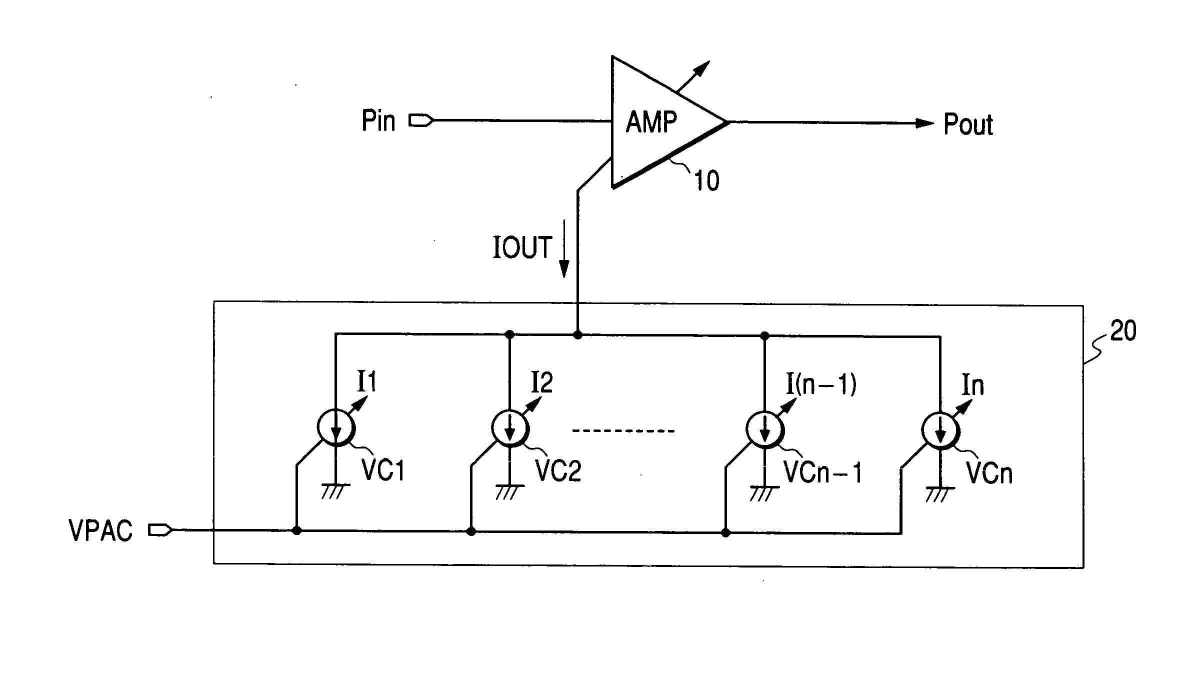
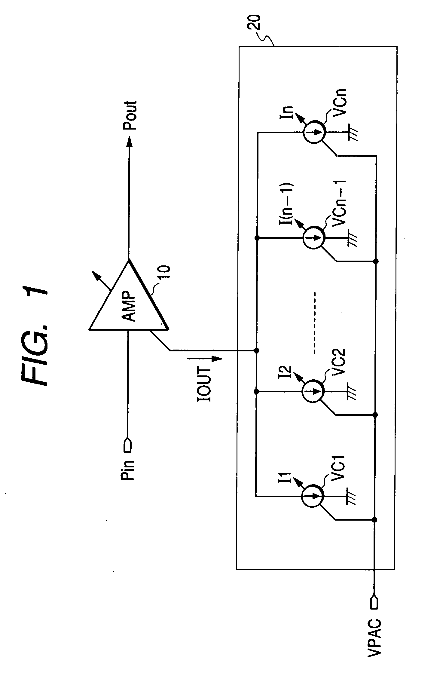
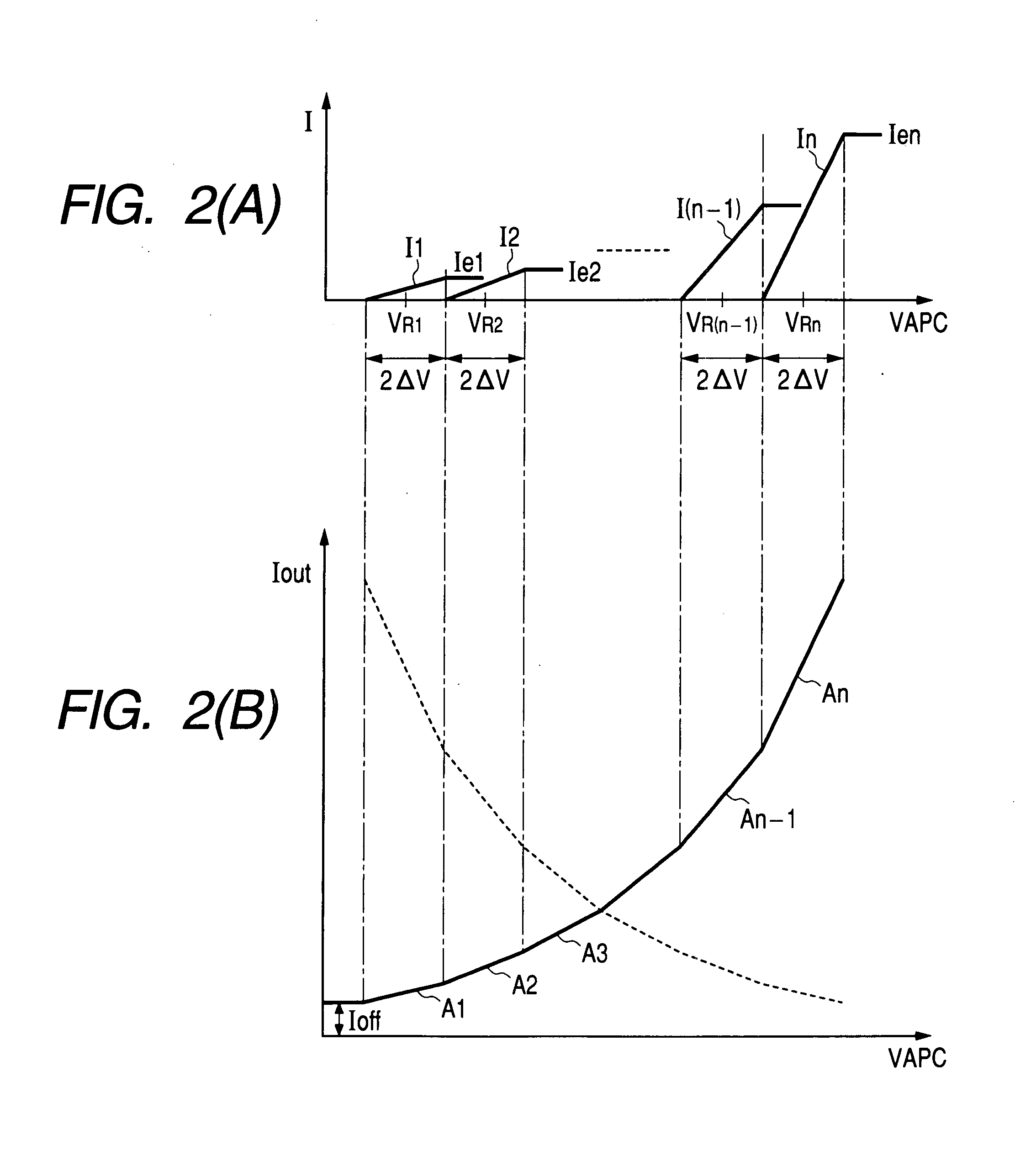
[0024]FIG. 1 schematically shows an embodiment of a bias circuit which generates a bias current supplied to a linear amplifier used as a gain control amplifier that constitutes a communication high-frequency power amplifier circuit. The bias circuit 20 according to the present embodiment is provided with a plurality of variable current sources VC1, VC2, . . . , VCn individually different in the magnitude of a current value and current start level. The bias circuit 20 is configured in such a manner that these variable current sources VC1, VC2, . . . , VCn are controlled based on an input control voltage VAPC to thereby combine their currents into a bias current, and the combined current varies exponentially with respect to the input control voltage VAPC.

[0025] Specifically described, the variable current sources VC1, VC2, . . . , VCn are respecti...


PUM


Abstract

The present invention provides a communication semiconductor integrated circuit device equipped with a high-frequency power amplifier circuit including a gain control amplifier and a bias circuit which supplies such a bias current as to linearly change the gain of the gain control amplifier, and a wireless communication system using the same. A bias current generating circuit which supplies a bias current to a linear amplifier that constitutes the communication high-frequency power amplifier circuit, comprises a plurality of variable current sources respectively different in current value and start level. These variable current sources are controlled according to an input control voltage and thereby combine their currents into a bias current. The combined bias current changes exponentially with respect to the input control voltage.

Description

CROSS-REFERENCES [0001] This is a continuation application of U.S. Ser. No. 10 / 836,197, filed on May 3, 2004, which is a continuation of U.S. Ser. No. 10 / 323,819, filed on Dec. 20, 2002 (now U.S. Pat. No. 6,750,719).BACKGROUND OF THE INVENTION [0002] This invention relates to a technology for enhancing controllability of output power based on a power control signal voltage of a high-frequency power amplifier circuit and gain's linear characteristics of a gain control amplifier, and particularly to a communication semiconductor integrated circuit device having a high-frequency power amplifier circuit built therein, and a technology effected if applied to a wireless communication system such as a cellular phone or the like with the communication semiconductor integrated circuit device built therein. [0003] A high-frequency power amplifier circuit has been built in an output unit provided on the transmitting side of a wireless communication system (mobile communication system) such as ...

Claims


Application Information

Patent Timeline
Patent Type & Authority Applications(United States)
IPC IPC(8): H03G3/10H03G1/00H03G3/30H04B1/04
CPCH03F1/0261H03F3/245H03F3/45085H03G2201/40H03G1/0023H03G3/3042H03G1/00
Inventor TOYOTA, KENJIHORI, KAZUAKIHIKASA, KAZUHIKO
Owner RENESAS ELECTRONICS CORP
Why Eureka
Try Eureka