Display and method for manufacturing display

a display and display technology, applied in the field of display, can solve problems such as the realization of large-scale and high-definition displays, and achieve the effect of suppressing streaks

Inactive Publication Date: 2008-01-31
SONY CORP
View PDF9 Cites 19 Cited by
  • Summary
  • Abstract
  • Description
  • Claims
  • Application Information

AI Technical Summary

Benefits of technology

0076]The embodiments of the present invention can suppress the occurrence of streaks attributed to differences in characteristics among transistors in a vertical scanner.
0077]Furthermore, the embodiments of th...

Problems solved by technology

The simple-matrix system has a simpler configuration but involves problems s...

Method used


Image

  • Display and method for manufacturing display
  • Display and method for manufacturing display
  • Display and method for manufacturing display

Examples


Embodiment Construction

[0109]Embodiments of the present invention will be described below in association with the drawings.

[0110]FIG. 13 is a diagram showing the configuration of an organic EL display that employs pixel circuits according to an embodiment of the present invention.

[0111]FIG. 14 is a diagram schematically showing an organic EL display panel according to an embodiment of the present invention.

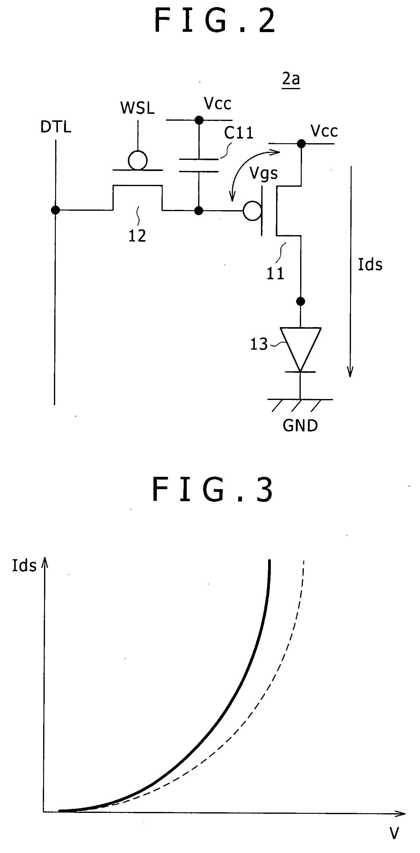
[0112]FIG. 15 is a circuit diagram showing the specific configuration of the pixel circuit according to the present embodiment.

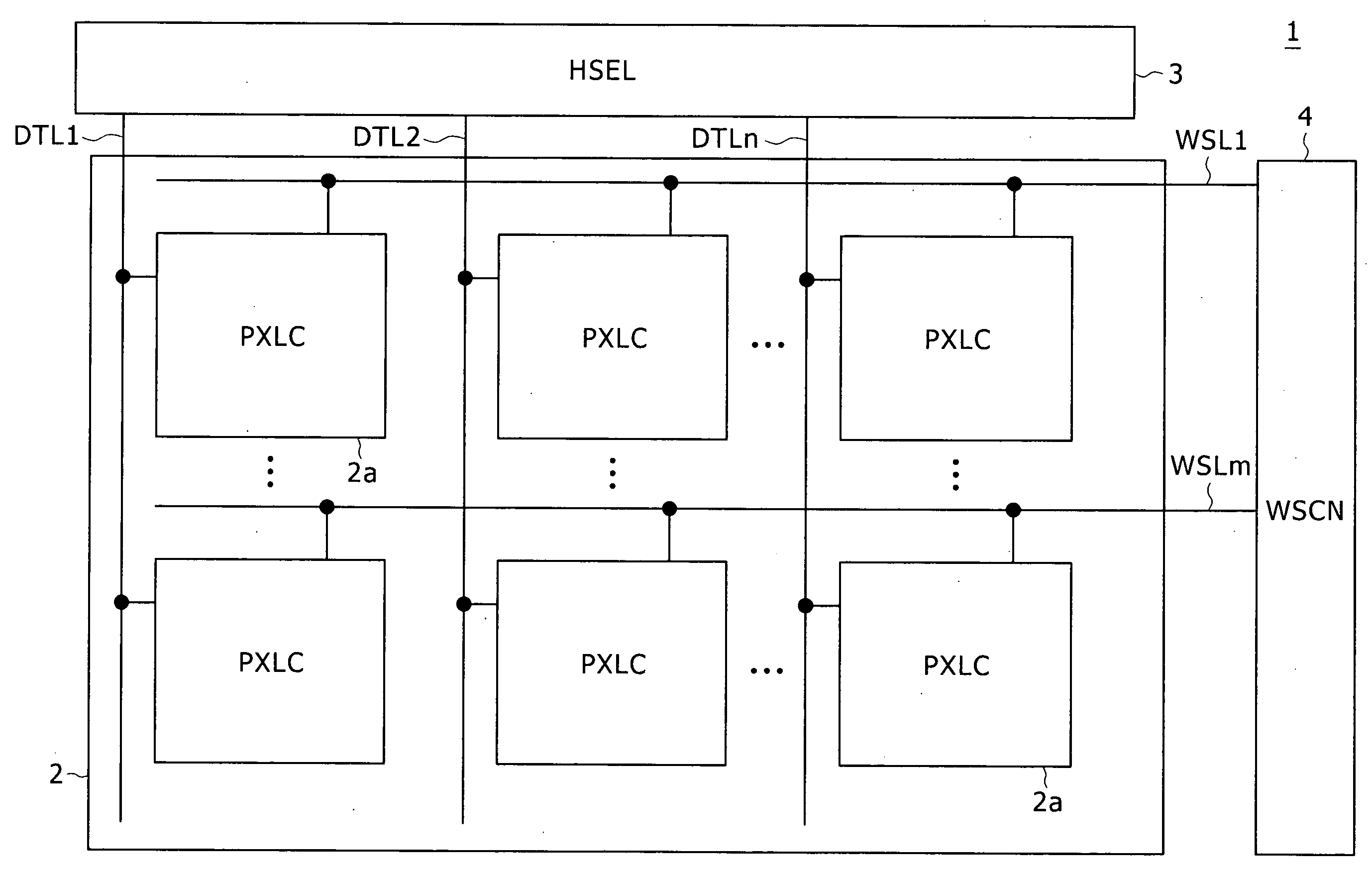
[0113]As shown in FIGS. 13 and 14, a display 100 includes a pixel array part 102 in which pixel circuits 101 are arranged in an m×n matrix, a horizontal selector (HSEL) 103, a write scanner (WSCN) 104, a drive scanner (DSCN) 105, a first auto-zero circuit (AZRD1) 106, and a second auto-zero circuit (AZRD2) 107. In addition, the display 100 includes also data lines DTL that are selected by the horizontal selector 103 and supplied with data signals in accordance with luminance inf...


PUM


Abstract

According to an embodiment of the present invention, there is provided a display that includes a pixel array part having a plurality of pixel circuits that are arranged in a matrix and each have at least one transistor of which conduction state is controlled through reception of a drive signal to a control terminal, and a scanner including a plurality of buffers that are formed of transistors. The buffers correspond to a pixel arrangement and output a drive signal to the control terminals of the transistors included in the pixel circuits. The transistors in the pixel circuits and the transistors in the buffers are formed through irradiation with laser light that is moved for scanning in a predetermined direction and has a predetermined wavelength. The transistors in the buffers are formed in such a way that the channel length direction of the transistors is set parallel to the scan direction of the laser light.

Description

CROSS REFERENCES TO RELATED APPLICATIONS[0001]The present invention contains subject matter related to Japanese Patent Application JP 2006-207446 and JP 2006-207447 filed in the Japan Patent Office on Jul. 31, 2006, the entire contents of which being incorporated herein by reference.BACKGROUND OF THE INVENTION[0002]1. Field of the Invention[0003]The present invention relates to a display in which pixel circuits each having an electro-optical element are arranged in a matrix, such as an organic electroluminescence (EL) display, and a method for manufacturing the same.[0004]2. Description of the Related Art[0005]In an image display, e.g., in a liquid crystal display, a large number of pixels are arranged in a matrix, and the light intensity is controlled on each pixel basis in accordance with information on an image to be displayed, to thereby display the image.[0006]This pixel-by-pixel control is implemented also in an organic EL display and the like similarly. The organic EL display...

Claims


Application Information

Patent Timeline
IPC IPC(8): G09G3/36G09G3/30
CPCG09G3/3233G09G3/30G09G3/3266G09G3/3291G09G5/10G09G2300/0417G09G2300/0452G09G2300/0819G09G2300/0842G09G2300/0861G09G2310/0262G09G2310/08G09G2320/0233G09G2320/043H01L27/124H01L27/1285H01L29/04H01L33/0041
Inventor MINAMI, TETSUOYAMASHITA, JUNICHIUCHINO, KATSUHIDE
Owner SONY CORP
Why Eureka
Try Eureka