Optical scanning device and image forming apparatus

a scanning device and image forming technology, applied in the direction of electrographic process apparatus, instruments, printing, etc., can solve the problems of increasing power consumption and noise, heat generation, degradation of durability, and unstable properties, and it is difficult to ensure the optical characteristics of the entire light flux

Active Publication Date: 2008-01-31
RICOH KK
View PDF4 Cites 57 Cited by
  • Summary
  • Abstract
  • Description
  • Claims
  • Application Information

AI Technical Summary

Problems solved by technology

With such means, however, there arise problems of increase in power consumption and noise, heat generation, and degradation of durability.
The light source including the light emitting points on one element, however, has some problems as follows:1. Heat generated by electrically driving light-emitting elements causes crosstalk between the light-emitting elements, and the crosstalk makes their property unstable.2. The more the number of light-emitting elements increases, the farther light emitting points are apart from the optical axis of an optical system.
Therefore, it is difficult to ensure optical characteristics for the entire light fluxes.
The technologies described in Japanese Patent Application Laid-Open Nos. 2001-272615 and 2001-350111 deals with the first problem, but both the patent documents do not teach or suggest the solution to the second problem.
As a result, a focus position changes, and a spot diameter thereby increases, resulting in image degradation.
As a result, image degradation is largely affected thereby.
However, this structure has a disadvantage such that the increase of the number of lenses causes cost increase.
Moreover, the technology described in Japanese Patent Application Laid-Open No. 2002-214556 also requires one piece of glass lens, and this is also a factor of cost increase.
However, the scanning lens has a wide area for passage of light flux, and the diffractive optical surface has to be formed on the wide area, which takes time, and this causes cost increase.
Therefore, higher machining technology is required for an area which is farther from the axis, and this may easily cause manufacturing error to occur.
If the manufacturing error occurs, then diffraction efficiency varies, which causes the light amount on the surface to be scanned to change for each light flux.
Thus, images provided by the image forming apparatus have non-uniform density.

Method used


Image

  • Optical scanning device and image forming apparatus
  • Optical scanning device and image forming apparatus
  • Optical scanning device and image forming apparatus

Examples


first embodiment

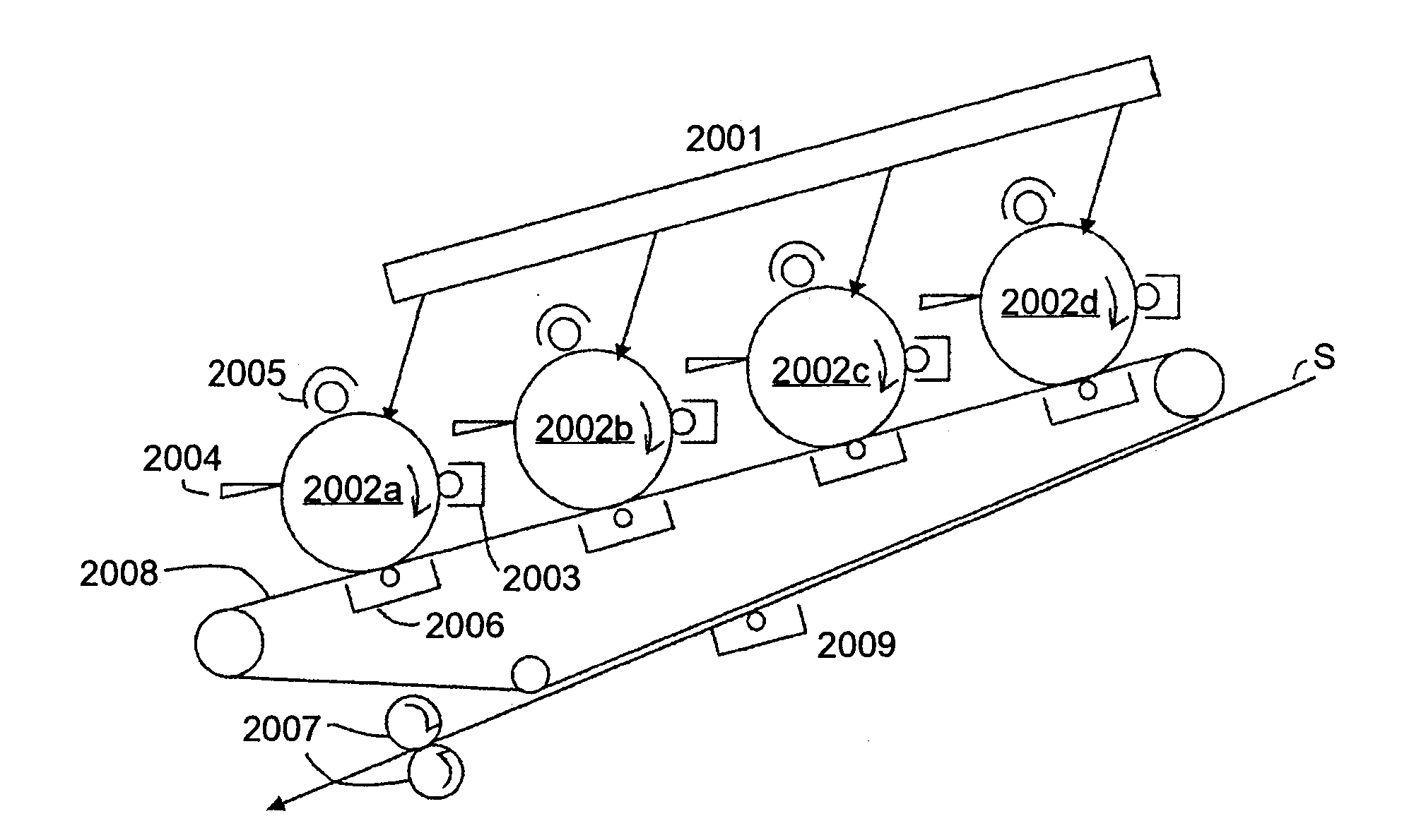
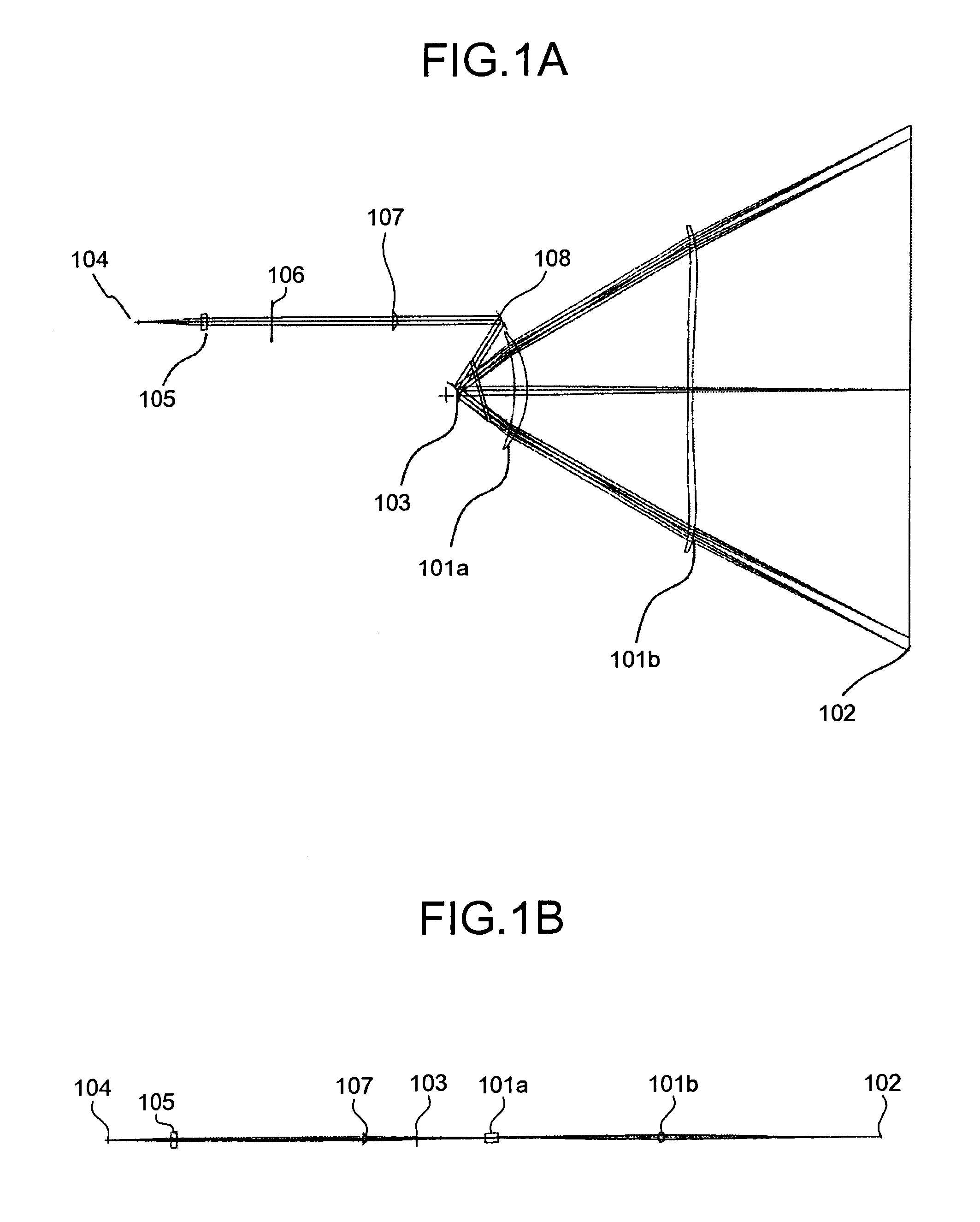
[0046]FIGS. 1A and 1B depict optical arrangement of an optical scanning device according to the present invention. More specifically, FIG. 1A depicts the optical arrangement in a main-scanning plane, and FIG. 1B depicts that in a sub-scanning plane. The optical scanning device has an incident optical system including a light source 104, a coupling lens 105, an aperture 106, and a linear-image forming lens 107. The optical scanning device also has a scanning optical system including a first scanning lens 101a and a second scanning lens 102b. An optical deflector 103 is provided between the incident optical system and the scanning optical system. An incident mirror 108 is arranged in the incident optical system to cause light flux to enter a deflection reflecting surface of the optical deflector 103 at an appropriate angle.

[0047]In FIGS. 1A and 1B, the coupling lens 105 couples divergent light beams emitted from the light source 104 into substantially parallel light flux for optical e...

third embodiment

[0071]FIGS. 8A and 8B represent modifications of the In FIG. 8A, the parallelograms each having the minimum area are indicated by the solid line and the dotted line, respectively. However, in both cases, there is no light emitting point at each acute angle of the two parallelograms. In this manner, the light emitting points helping the optical scanning are not provided near locations of the vertexes of the acute angles, among the vertexes of the parallelogram, i.e., locations arranged farthest from the optical axis. Therefore, the light beams such that intervals between scanning lines easily vary can be removed, and thus satisfactory optical scanning can be performed with any ones of the light fluxes. The light emitting point to be removed may be one point on each acute angle of the parallelogram (see FIG. 8A), or a plurality of points around each acute angle may be removed (see FIGS. 7 and 8B). The parallelogram surrounding the light emitting points may be one being long in the ma...

fourth embodiment

[0086]The light source 1 (1′) is a semiconductor laser with a light emission wavelength of 655 nanometers in design. If the temperature rises 1° C. from a reference temperature of 25° C., then the light emission wavelength shifts to the long wavelength side by 0.20 nanometer. As for the mode hopping, as explained above, it is assumed that the wavelength change is 0.8 nanometer. In the fourth embodiment, as shown in FIG. 10, two semiconductor lasers each having one light emitting point are provided. However, a semiconductor laser array or a VCSEL array can also be used.

[0087]Coupling Lens

[0088]The coupling lens 2 (2′) is a glass lens as explained above, and is disposed so that the lens has a focal length of 15 millimeters and has a function of converting the light beam to substantially parallel light beam. The aspheric surface is used for both surfaces of the coupling lens 2 (2′), so that the aspheric surfaces satisfactorily correct the wavefront aberration of coupled light beam alth...


PUM


Abstract

An optical scanning device includes a light source having light emitting points for emitting light beams, a coupling optical element that couples the light beams, a deflecting unit that deflects and scans the light beams, and a scanning optical system that focus the light beams to form an image. The optical scanning device satisfies the following condition:F tan(θ / 2)+A<D / 0.7 where A is the maximum distance between the light emitting points and an optical axis of the coupling optical element, θ is a divergence angle (full-width half-maximum) of the light beams, F is a focal length of the coupling optical element, and D is an effective radius of the coupling optical element.

Description

CROSS-REFERENCE TO RELATED APPLICATIONS[0001]The present application claims priority to and incorporates by reference the entire contents of Japanese priority document, 2006-205095 filed in Japan on Jul. 27, 2006 and 2007-126319 filed in Japan on May 11, 2007.BACKGROUND OF THE INVENTION[0002]1. Field of the Invention[0003]The present invention relates to an optical scanning device and an image forming apparatus.[0004]2. Description of the Related Art[0005]In image forming apparatuses such as digital copiers and laser printers, high-density image formation using optical scanning has been progressing, and a small-sized beam spot on a photosensitive element is demanded of the image forming apparatus to meet the progress. In addition, there is a continuous demand for high-speed image formation, and thus it is desired to realize an optical scanning device capable of meeting these demands. As a means to achieve high-speed and high-density image formation, rotation speed of a polygon scann...

Claims


Application Information

Patent Timeline
Patent Type & Authority Applications(United States)
IPC IPC(8): G03G15/045G02B26/08
CPCG02B13/0005G02B26/125G03G15/326G03G15/0435B41J2/455B41J2/473G03G2215/0404
Inventor ICHII, DAISUKEHAYASHI, YOSHINORIUEDA, TAKESHISAKAI, KOHJISAISHO, KENICHIRO
Owner RICOH KK
Why Eureka
Try Eureka