Interposer structures and methods of manufacturing the same

Inactive Publication Date: 2008-02-07
GLOBALFOUNDRIES INC
View PDF6 Cites 6 Cited by
  • Summary
  • Abstract
  • Description
  • Claims
  • Application Information

AI Technical Summary

Benefits of technology

[0012] The present invention provides structures for interposers for use with rigid or flexib

Problems solved by technology

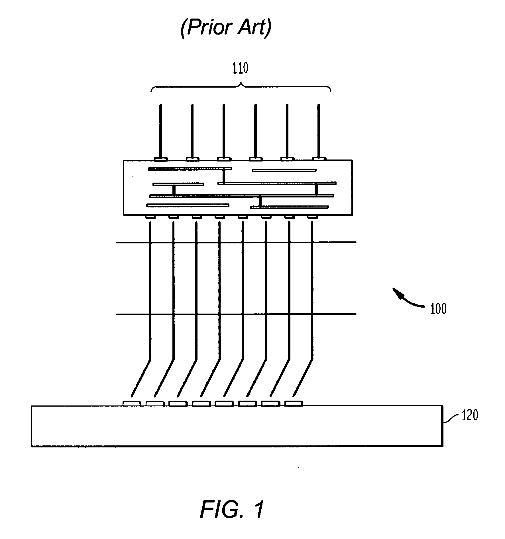
One key factor in determining the method of testing the dies is the complexity of the device design.
The number of input and output (I/O) pads present on a die is often indicative of the complexity of the design, wherein a higher number of I/O pads is attributed to higher design complexity.
For a die with a high number of I/O pads, i.e., those having hundreds to thousands of I/O pads typically in an aerial array, customized probe cards connecting the die to a teste

Method used


Image

  • Interposer structures and methods of manufacturing the same
  • Interposer structures and methods of manufacturing the same
  • Interposer structures and methods of manufacturing the same

Examples


Embodiment Construction

[0091] Electroless plating refers to the autocatalytic reduction of a metal ion at a cathodic surface. The metal ion in solution reduces at the surface of the work piece through a parallel oxidation reaction. For example, a hypophosphite anion can be oxidized according to the following reaction: Ni2++2⁢ ⁢e-->Ni0H2⁢PO2-+H2⁢O->H2⁢PO3-+2⁢ ⁢H++2⁢ ⁢e-Ni2++H2⁢PO2-+H2⁢O->Ni(metal)+2⁢ ⁢H++H2⁢PO3-(Equation⁢ ⁢1)

[0092] Equation 1 renders hydrogen evolution as a result of the plating process. Excess hydrogen production can interfere with the quality of the plated film, however, and should be avoided by proper bath agitation and / or additions of surface dewetting agents. Commercially available electroless solutions contain stabilizers to control the reaction rates of Equation 1. Electroless plating baths also contain various metal salts, reducing agents and organics to buffer and maintain the solution as well as to adjust properties such as hardness and the appearance of deposits in the plating ...


PUM


Abstract

Flexible and rigid interposers for use in the semiconductor industry and methods for manufacturing the same are described, Auto-catalytic processes are used to minimize the costs associated with the production of flexible interposers, while increasing the yield and lifetime. Electrical contact regions are easily isolated and the risk of corrosion is reduced because all portions of the interposer are plated at once. Leads projecting from the flexible portion of the interposers accommodate a greater variety of components to be tested. Rigid interposers include a pin projecting from a probe pad affixed to a substrate. The rigidity of the pin penetrates oxides on a contact pad to be tested. Readily available semiconductor materials and processes are used to manufacture the flexible and rigid interposers according to the invention. The flexible and rigid interposers can accommodate pitches down to 25 μm.

Description

RELATED APPLICATIONS [0001] This application is a continuation-in-part of, and claims priority to, co-pending U.S. patent application Ser. No. 10 / 909,111, filed on Jul. 30, 2004.FIELD OF THE INVENTION [0002] This invention relates to interposer structures used in probing semiconductor wafers and methods of fabricating the same. BACKGROUND OF THE INVENTION [0003] One of the final stages in the fabrication of integrated circuits on semiconductor wafers is testing and sorting of the functionality of the individual semiconductor chips, the dies. The purpose of testing the dies is to determine if the dies function as they were designed for; i.e., whether the dies produce intended outputs for given inputs. Once functionality is established, the dies are sorted for operating frequency, i.e., the dies are ranked in terms of how fast each die operates. Due to the variations in processing steps, different dies function at different speeds. [0004] There are a variety of techniques employed for...

Claims


Application Information

Patent Timeline
IPC IPC(8): G01R31/02
CPCG01R1/0735G01R3/00H05K3/4038H05K3/4007H05K3/06
Inventor CORDES, STEVEN A.FARINELLI, MATTHEW J.GOMA, SHERIF A.
Owner GLOBALFOUNDRIES INC
Why Eureka
Try Eureka