

Method and Apparatus for the Etching of Microstructures
a microstructure and etching technology, applied in the field of microstructure manufacturing, can solve the problems of reducing the efficiency of the apparatus, posing a significant safety hazard to users, lack of control of the etching process, etc., and achieves the effect of increasing the rate of etching and partial pressure of the etching material vapour
- Summary
- Abstract
- Description
- Claims
- Application Information
AI Technical Summary
Benefits of technology
Problems solved by technology
Method used
Image

Examples
Embodiment Construction
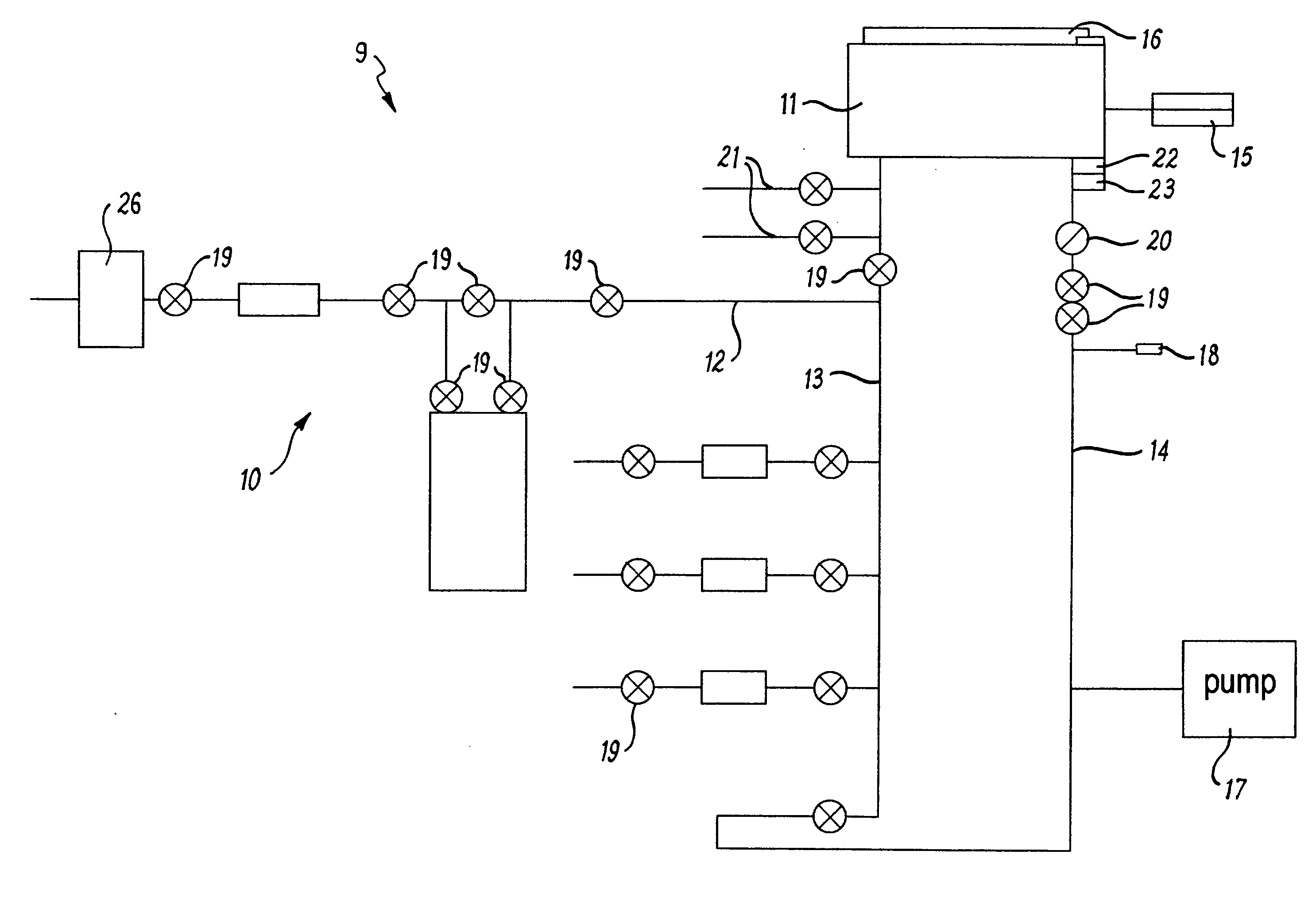
[0106] Referring initially to FIG. 3 a schematic representation of a gas phase etching apparatus 9, employed for the manufacture of micro electromechanical microstructures (MEMS) is presented in accordance with an aspect of the present invention. The gas phase etching apparatus 9 can be seen to comprise an etching gas source, depicted generally at 10 and shown in further detail within FIG. 4, and a process chamber, depicted generally at 11 and shown in further detail within FIG. 5.
[0107] The etching gas source 10 is employed to provide the required XeF2 etching gas to the process chamber 11 via a first gas supply line 12 and a process chamber input line 13. Also coupled to the process chamber 11 is a pumping line 14 and a first pressure gauge 15 that provides a means for determining the pressure within the process chamber 11. The process chamber 11 can be seen to further comprise a lid 16 that provides a means of access to the chamber 11 so as to allow for the loading and unloading...
PUM
| Property | Measurement | Unit |
|---|---|---|
| Partial vapour pressure | aaaaa | aaaaa |
| volume ratio | aaaaa | aaaaa |
| volume ratio | aaaaa | aaaaa |
Abstract
Description
Claims
Application Information