Thin-film transistor substrate, method of manufacturing the same and display apparatus having the same

a thin film transistor and substrate technology, applied in the field of display apparatus, can solve the problems of affecting emulating impurities from the organic insulating layer, and reducing the display quality of the lcd apparatus, so as to prevent damage to the lower organic layer, reduce the effect of afterimages, and enhance the display

Active Publication Date: 2008-02-21
SAMSUNG DISPLAY CO LTD
View PDF4 Cites 18 Cited by
  • Summary
  • Abstract
  • Description
  • Claims
  • Application Information

AI Technical Summary

Benefits of technology

[0012]According to an aspect of the present invention, an inorganic insulating layer is disposed on an organic layer. Thus, impurities from the organic layer may be blocked, so that liquid crystal may be prevented from being contaminated and display defects, such as afterimages, may be reduced.
[0013]According to a method of manufacturing a TFT substrate of the present invention, an inorganic insulating layer is formed at a low temperature of about 100° C. to about 250° C. Thus, damage to a lower organic layer may be prevented and display properties may be enhanced.
[0014]Additionally, according to a method of manufacturing a TFT substrate of the present invention, manufacturing time may be shortened by forming an inorganic insulating layer having a precise thickness.

Problems solved by technology

When the TFT substrate and the common electrode substrate are misaligned during the manufacturing process for the LCD apparatus, the display quality of the LCD apparatus is adversely affected.
However, impurities from the color filter may elute through a gap or an opening between pixel electrodes, contaminate the liquid crystal and cause an afterimage to be displayed.
Furthermore, when an organic insulating layer is used as a planarization layer under the pixel electrode, impurities from the organic insulating layer elute.
As a result, the liquid crystal is also contaminated, and the afterimage increases.

Method used


Image

  • Thin-film transistor substrate, method of manufacturing the same and display apparatus having the same
  • Thin-film transistor substrate, method of manufacturing the same and display apparatus having the same
  • Thin-film transistor substrate, method of manufacturing the same and display apparatus having the same

Examples


Embodiment Construction

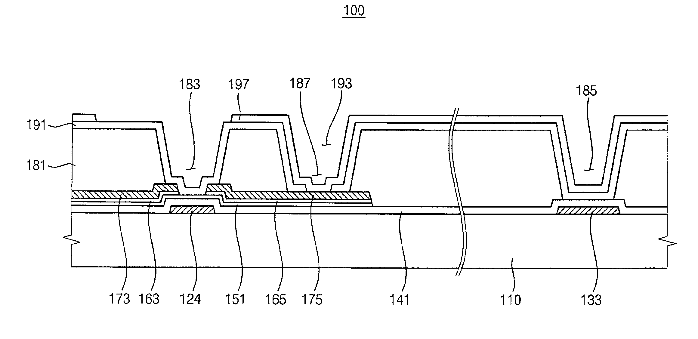
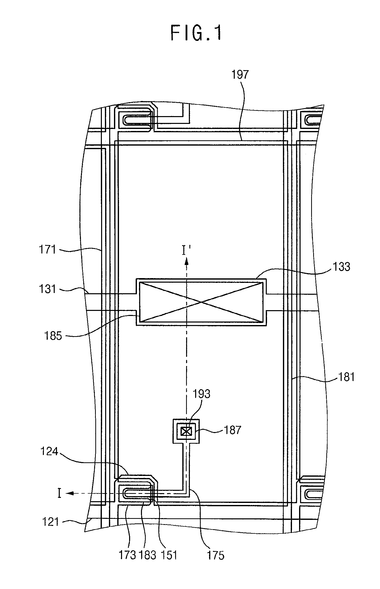
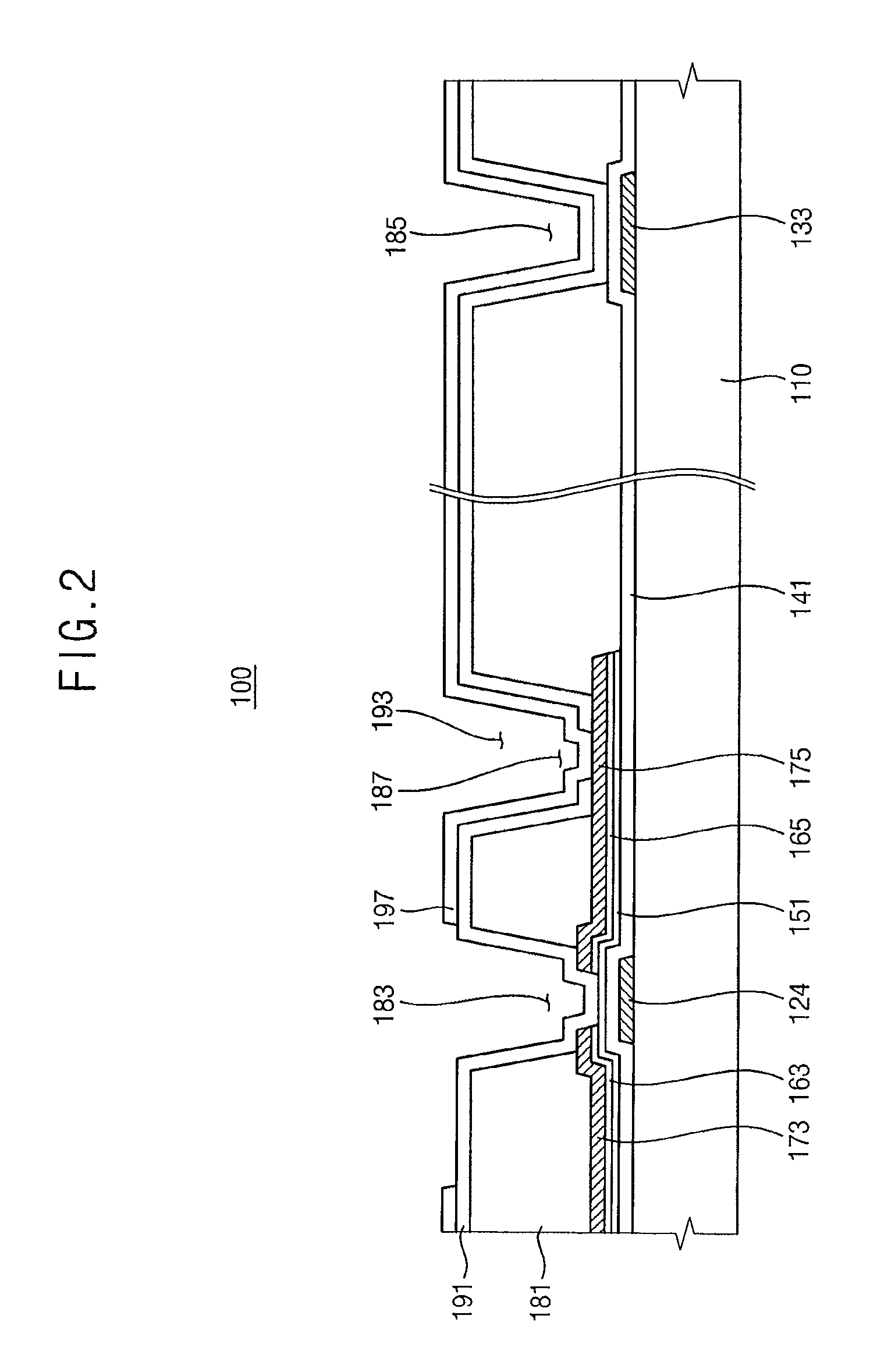
[0024]It will be understood that when an element or layer is referred to as being “on,”“connected to” or “coupled to” another element or layer, it can be directly on, connected or coupled to the other element or layer or intervening elements or layers may be present. In contrast, when an element is referred to as being “directly on,”“directly connected to” or “directly coupled to” another element or layer, there are no intervening elements or layers present.

[0025]Embodiments of the invention are described herein with reference to cross-section illustrations that are schematic illustrations of idealized embodiments (and intermediate structures) of the invention. As such, variations from the shapes of the illustrations as a result, for example, of manufacturing techniques and / or tolerances, are to be expected. Thus, embodiments of the invention should not be construed as limited to the particular shapes of regions illustrated herein but are to include deviations in shapes that result,...


PUM


Abstract

In a thin-film transistor (TFT) substrate, a gate insulating layer is disposed on a gate electrode electrically connected to a gate line. A semiconductor layer is disposed on the gate insulating layer. A source electrode is electrically connected to a data line that intersects the gate line. A drain electrode faces the source electrode and defines a channel area of a semiconductor layer. An organic layer is disposed on the data line and has a first opening exposing the channel area. An inorganic insulating layer is disposed on the organic layer. A pixel electrode is disposed on the inorganic insulating layer and electrically connected to the drain electrode. The inorganic insulating layer covers the first opening, and thickness of the inorganic insulating layer is substantially uniform.

Description

CROSS-REFERENCE TO RELATED APPLICATIONS[0001]This application claims priority under 35 U.S.C. §119 to Korean Patent Application No. 2006-77931, filed on Aug. 18, 2006 in the Korean Intellectual Property Office (KIPO), the contents of which are herein incorporated by reference in their entirety.BACKGROUND OF THE INVENTION[0002]1. Field of the Invention[0003]The present invention relates to a display apparatus and, more particularly, to a TFT substrate, a method of manufacturing the TFT substrate and a display apparatus having the TFT substrate.[0004]2. Description of the Related Art[0005]Recently, flat panel display apparatus, such as the organic light-emitting display (OLED), the plasma display panel (PDPs) and the liquid crystal display (LCD) have been developed to substitute for heavy and large cathode ray tube (CRT) displays. The PDP apparatus displays images using plasma generated by an electric discharge. The OLED apparatus displays images and characters using organic electrolu...

Claims


Application Information

Patent Timeline
Patent Type & Authority Applications(United States)
IPC IPC(8): H01L27/12H01L21/84
CPCG02F1/136227H01L27/3258G02F2001/136222G02F1/136222H10K59/124
Inventor RYU, HYE-YOUNGKIM, JANG-SOOKANG, SU-HYOUNG
Owner SAMSUNG DISPLAY CO LTD
Why Eureka
Try Eureka