Field emission system and method for improving its vacuum

a field emission system and vacuum technology, applied in the direction of discharge tube/lamp details, discharge tube main electrodes, discharge tubes luminescnet screens, etc., can solve the problems of reducing the field emission performance caused by ion bombardment, the shape of the emitter tip gradually deteriorates, and the decrease of the field emission performance almost unavoidable, so as to facilitate mass production of field emission display devices, reduce the effect of fabricating cost and reducing the thickness and weight of the system

Inactive Publication Date: 2008-02-21
IND TECH RES INST
View PDF2 Cites 10 Cited by
  • Summary
  • Abstract
  • Description
  • Claims
  • Application Information

AI Technical Summary

Benefits of technology

[0012]The method for improving vacuum of the field emission system of the present invention can be integrated in standard processes of field emission display devices without additional fabricating steps, thus facilitating mass production of the field emission display devices. Moreover, it is unnecessary to add a getter device to the present field emission system. The fabricating cost can be reduced. The system's thickness and weight also can be decreased.

Problems solved by technology

Under the influence of ion bombardment, the shape of the emitter tip is gradually deteriorated, and the distribution of electric field is affected.
Therefore, the decrease of the field emission performance caused by ion bombardment is almost unavoidable.
The higher the vacuum level is, the less the residual gas is, and ion bombardment becomes weaker.
The vacuum level of the field emission display device is limited.

Method used


Image

  • Field emission system and method for improving its vacuum
  • Field emission system and method for improving its vacuum
  • Field emission system and method for improving its vacuum

Examples


first embodiment

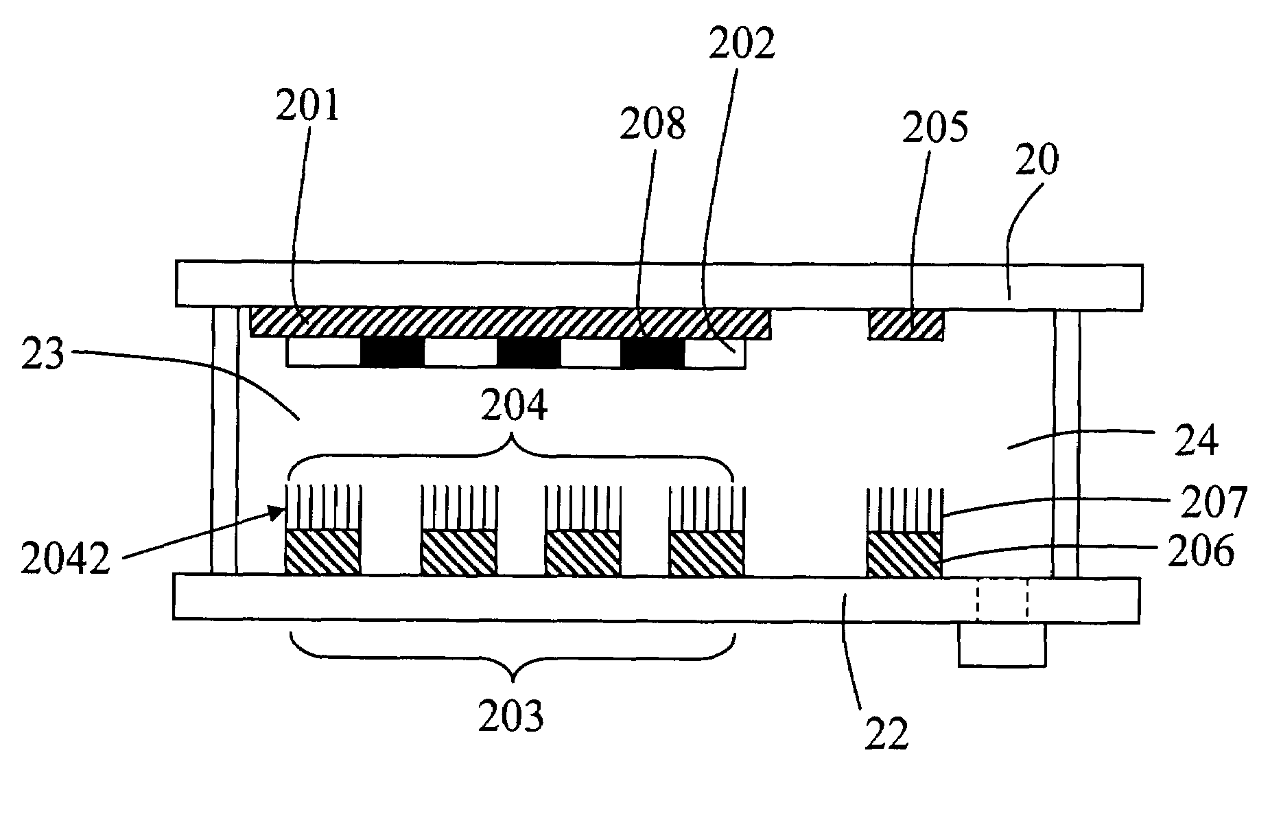
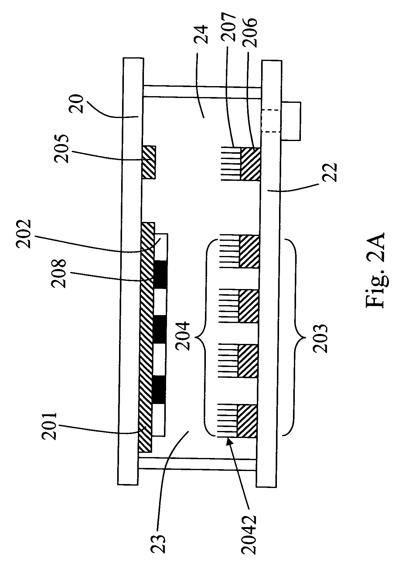
[0025]Before sealing the panel of the field emission display of the first embodiment, the aging process is performed unto the carbon nanotube units 2042 in the display area 23 and the carbon nanotubes 207 in the getter area 24 such that the gases bonding to the surfaces of the carbon nanotubes and accumulated in the interstices of the stacking carbon nanotubes are released, and the carbon nanotubes 207 in the getter area 24 become surface-unsaturated absorbing material. The residual gas within the system is exhausted by a vacuum system, and then the panel is sealed. While the field emission display is operated, voltage is not applied to the second anode wire 205 and the second cathode wire 206 of the getter area 24. As such, the carbon nanotubes 207 are only functioned as getter agent but do not provide field emission.

[0026]In addition, the surface-unsaturated carbon nanotubes also can be formed on other non-display areas such as the inner surface areas of the lower substrate 22 cor...

third embodiment

[0029]Similarly, before sealing the panel of the field emission display device of the third embodiment, the aging process is performed unto the carbon nanotube units 305 in the display area 33 and the carbon nanotubes 309 in the getter area 34 such that the gases bonding to the surfaces of the carbon nanotubes and accumulated in the interstices of the stacking carbon nanotubes are released, and the carbon nanotubes 309 in the getter area 34 become surface-unsaturated absorbing material. The residual gas within the system is exhausted by the vacuum system, and then the panel is sealed. While the field emission display device is operated, the voltage is not applied to the second anode wire 307 and the second cathode wire 308 of the getter area 34. Thus, the carbon nanotubes 309 are only functioned as getter agent but do not provide field emission. Alternatively, the carbon nanotubes 309 in the getter area 34 also can grow on the second anode wire 307.

[0030]The geometric shape of the g...


PUM


Abstract

The present invention provides a field emission system and a method for improving its vacuum. The present invention employs aging surface-unsaturated carbon nanotubes in non-display areas of the field emission system as getter material to absorb residual gas within the system so as to improve its vacuum. The present method for improving vacuum of the field emission system can be integrated with the standard process of a field emission display device without additional fabricating steps, and thus facilitating the mass production of the field emission display device.

Description

BACKGROUND OF THE INVENTION[0001]1. Field of the Invention[0002]The present invention relates to a field emission system and a method for improving its vacuum, and more particularly, to a field emission system employing surface-unsaturated nanomaterial as getter material.[0003]2. Description of Related Art[0004]In field emission display (FED) devices, each pixel contains several hundreds to thousands of micro-tip emitters or cabon nanotubes (CNTs) formed on a back plate of the field emission display device to serve as electron emission sources, and a phosphor layer emitting light by way of being bombarded by electrons from the electron emission sources is formed on a front plate of the field emission display device. A gap between the front plate and the back plate of the field emission display device is usually about 200 μm to several millimeters (mms). The display must be maintained in a high vacuum level so that electrons move without energy loss.[0005]FIG. 1 is a schematic cross-...

Claims


Application Information

Patent Timeline
Patent Type & Authority Applications(United States)
IPC IPC(8): H01J63/04H01J1/62
CPCH01J7/18H01J29/94H01J2329/948H01J61/26H01J63/02H01J31/127
Inventor CHIEN, YU-HANPENG, CHIH-PINGFU, CHUAN-HSULIN, WEI-YICHAN, LIH-HSIUNG
Owner IND TECH RES INST
Why Eureka
Try Eureka