Inductor circuit board, method of forming inductor, and bias-T circuit

Inactive Publication Date: 2008-02-21
FUJITSU LTD
View PDF3 Cites 17 Cited by
  • Summary
  • Abstract
  • Description
  • Claims
  • Application Information

AI Technical Summary

Benefits of technology

[0038]Another object of the present invention is to provide a method of forming an inductor, whi

Problems solved by technology

This makes it impossible to directly use such a surface-mount inductor as described above in the transmission line, and it is necessary to make the inductor compatible with broadband.
However, actually, it is impossible to use an inductor formed simply by connecting the component inductors in series (hereinafter referred to as “the series inductor”) since the characteristics thereof are degraded e.g. due to occurrence of a parasitic capacitance of the inductor.
However, the above state is an ideal one, and in the actual high-frequency circuit, parasitic capacitances of the component inductors themselves and earth capacitances cannot be ignored.
This makes it impossible for a mere series inductor to be compatible with broad

Method used


Image

  • Inductor circuit board, method of forming inductor, and bias-T circuit
  • Inductor circuit board, method of forming inductor, and bias-T circuit
  • Inductor circuit board, method of forming inductor, and bias-T circuit

Examples


Example

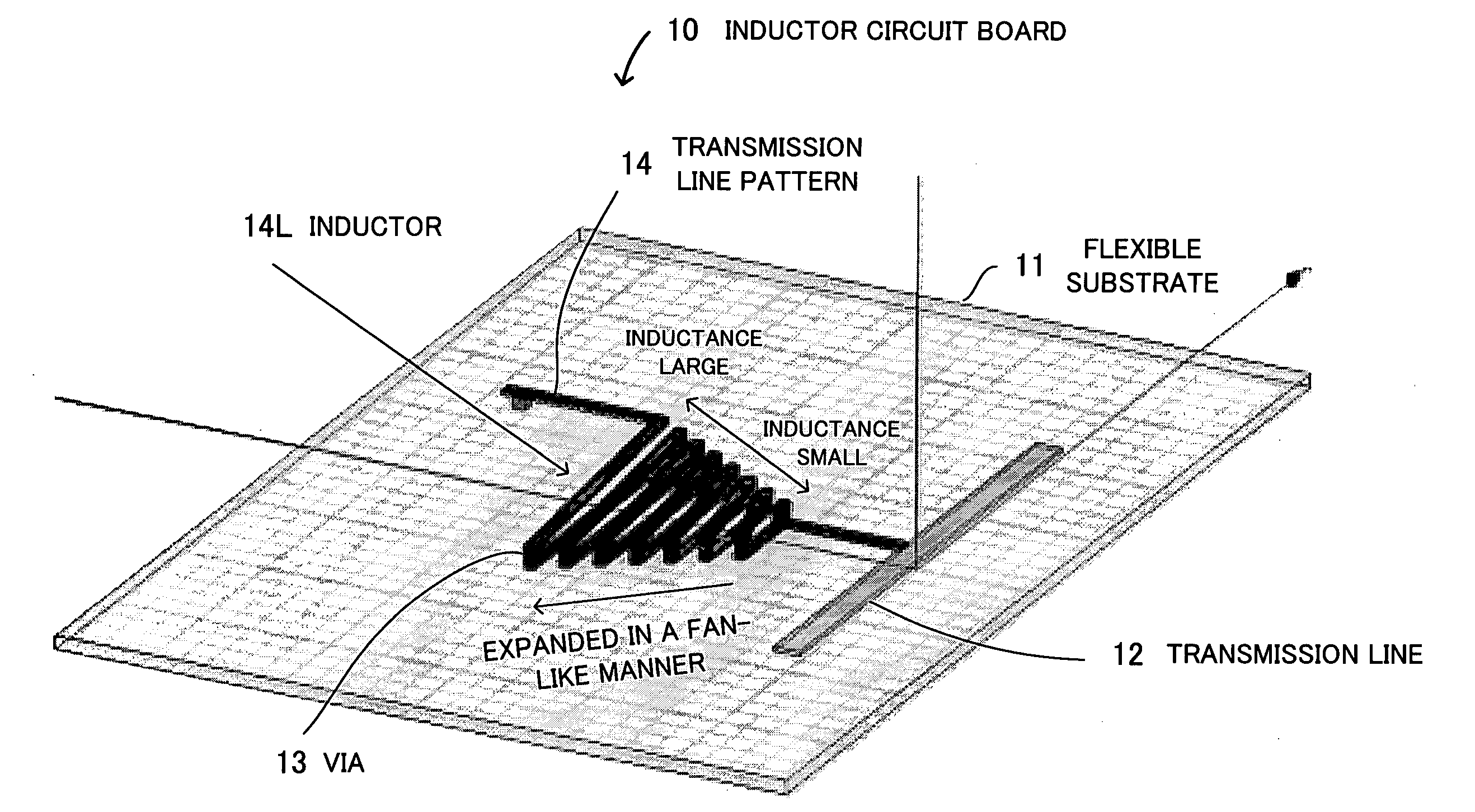
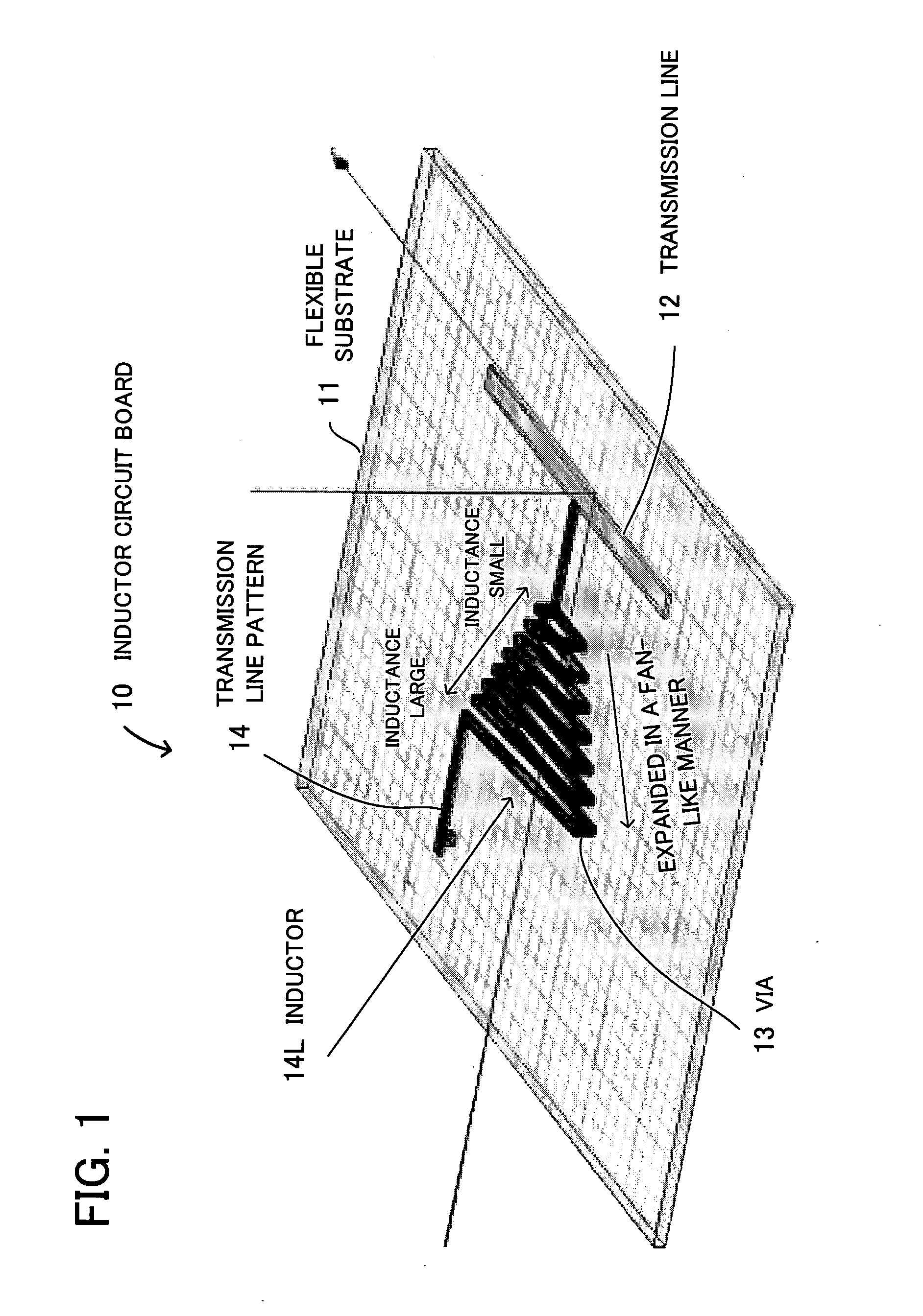
[0065]The invention will now be described in detail with reference to the drawings showing a preferred embodiment thereof. FIG. 1 is a diagram of an inductor circuit board. The inductor circuit board 10 is a flexible printed circuit (FPC) and is comprised of a substrate (hereinafter referred to as “the flexible substrate”) 11 formed of polyimide, liquid polymer or a like material, a transmission line 12 formed on the flexible substrate 11, and an inductor 14L formed according to a transmission line pattern 14.

[0066]It should be noted that flexible printed circuits (FPCs) are printed circuit boards having flexibility, and due to bendability thereof, they are widely used in various small-sized products, such as cellular phones, digital cameras, and so forth, which are limited in mounting space.

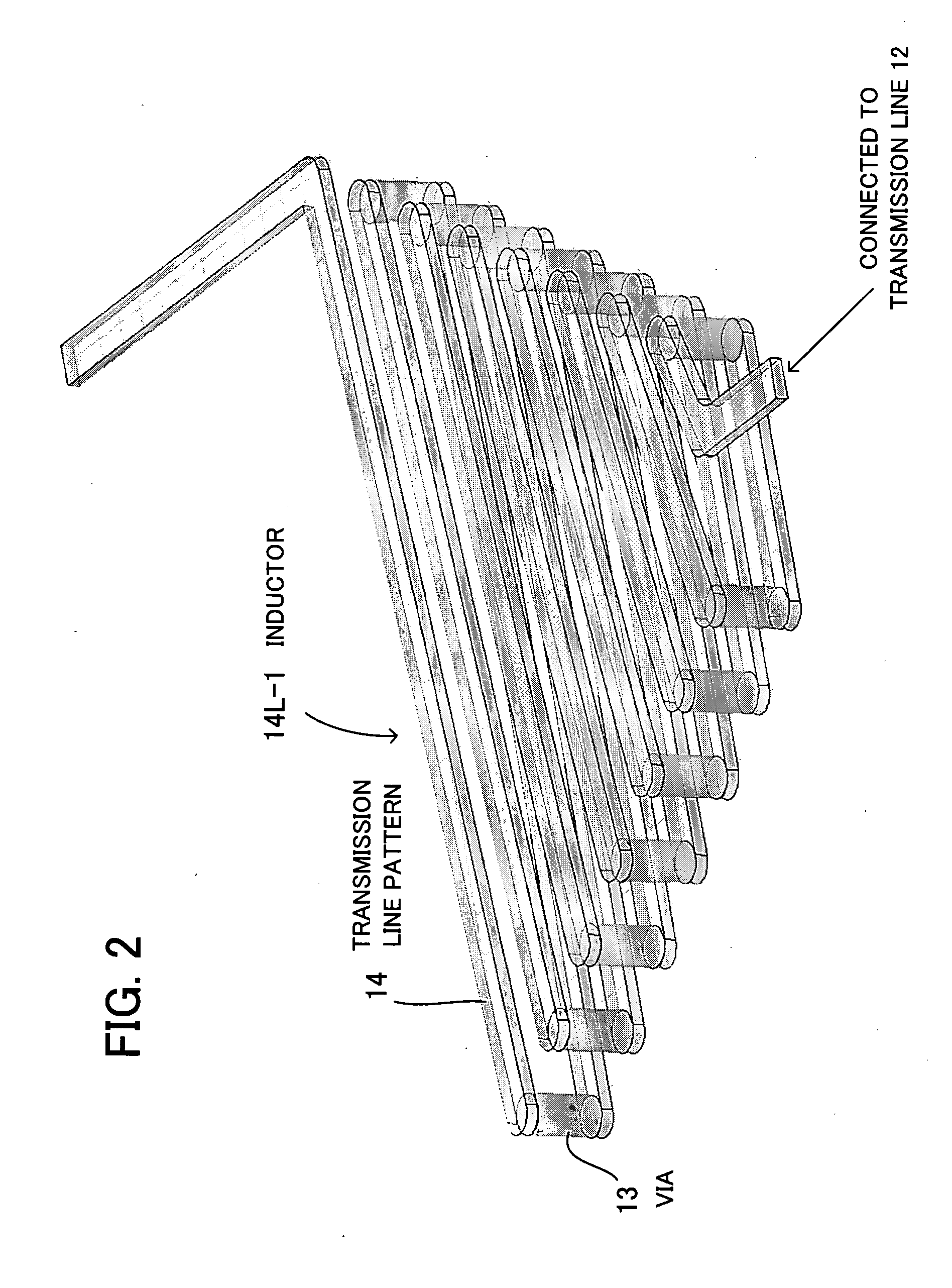
[0067]The inductor 14L formed according to the transmission line pattern 14 has a three-dimensional conical structure in which component inductors having different inductances are continuously c...


PUM


Abstract

An inductor circuit board that is made compatible with broadband by reducing parasitic capacitance of an inductor. The inductor circuit board is comprised of a flexible substrate made of a material, such as polyimide or liquid polymer, a transmission line formed on the flexible substrate, and an inductor. The inductor has a three-dimensional conical structure in which component inductors having different inductances are continuously connected to each other, with one end thereof connected to a portion of the transmission line between an input end and an output end thereof, and is formed according to a transmission line pattern by wiring on a plurality of surface layers of the flexible substrate and connecting portions wired on the surface layers by vias that connect between the layer surfaces of the substrate, such that the inductor is expanded in a fan-like manner as it is farther from the one end connected to the transmission line. A portion of the indictor closer to the transmission line has a smaller inductance, and a portion of the same farther from the transmission line has a larger inductance.

Description

CROSS-REFERENCE TO RELATED APPLICATIONS[0001]This application is based upon and claims the benefits of priority from the prior Japanese Patent Application No. 2006-222069 filed on Aug. 16, 2006, the entire contents of which are incorporated herein by reference.BACKGROUND OF THE INVENTION[0002]1. Field of the Invention[0003]This invention relates to an inductor circuit board, a method of forming an inductor, and a bias-T circuit, and more particularly to an inductor circuit board having an inductor wired on a circuit board for a high-frequency transmission application, such as 40 Gb / s, a method of forming an inductor on a circuit board for a high-frequency transmission application, and a bias-T circuit that supplies a high-frequency signal by superposing a DC component thereon.[0004]2. Description of the Related Art[0005]Recently, with the development of multi-media technology, there is an increasing demand for constructing optical communication networks that transmit high-speed, lar...

Claims


Application Information

Patent Timeline
IPC IPC(8): H01P1/00
CPCH01F27/34H01F2005/006H01P1/2007H05K1/0237H05K1/0393H05K1/165H05K2201/097H01F17/0006H01F2017/0073H01F17/04H01F2017/006
Inventor YAGISAWA, TAKATOSHI
Owner FUJITSU LTD
Why Eureka
Try Eureka