Gan-Based Light-Emitting Element and Method for Producing Same

a technology of light-emitting elements and gan-based compound semiconductor layers, which is applied in the direction of semiconductor/solid-state device manufacturing, semiconductor devices, electrical devices, etc., can solve the problems of increasing operating voltage, reducing luminous efficiency, and saturation of luminance, so as to prevent the occurrence of phenomena, reduce the crystal defect density, and reduce the resulting crystal defect density

Inactive Publication Date: 2008-02-28
SONY CORP
View PDF11 Cites 12 Cited by
  • Summary
  • Abstract
  • Description
  • Claims
  • Application Information

AI Technical Summary

Benefits of technology

[0075] In the method for producing the GaN-based semiconductor light-emitting element, the first underlying GaN-based compound semiconductor layers are formed by lateral epitaxial growth from the seed layers; hence, basically, the first underlying GaN-based compound semiconductor layers each having an extremely low crystal defect density can be obtained. However, the crystal defect density of a portion of each of the first underlying GaN-based compound semiconductor layers grown on the seed layers is high. Thus, in the method for producing the GaN-based semiconductor light-emitting element, the second underlying GaN-based compound semiconductor layers are formed on top faces of the first underlying GaN-based compound semiconductor layers while top faces of the high-crystal-defect-density portions of the first underlying GaN-based compound semiconductor layers grown on the seed layers are covered with the mask layers. As a result, the crystal defect density in the resulting second underlying GaN-based compound semiconductor layers is extremely low as a whole.
[0076] Furthermore, the top face of each of the resulting second underlying GaN-based compound semiconductor layers is parallel to the a-plane, the m-plane, or the nonpolar plane. The side face thereof corresponds to the c-plane or the like. Accordingly, in each of the first GaN-based compound semiconductor layer, the active layer composed of a GaN-based compound semiconductor, the second GaN-based compound semiconductor layer, and the contact layer formed in that order on the second underlying GaN-based compound semiconductor layers, the top face thereof is parallel to the a-plane, the m-plane, or the nonpolar plane. The side face (for example, c-plane) is perpendicular to the interfaces. Thus, even when piezoelectric spontaneous polarization occurs in the active layer, piezoelectric spontaneous polarization does not occur in the thickness direction of the active layer but occurs in the direction substantially perpendicular to the thickness direction of the active layer. Therefore, it is possible to prevent the occurrence of phenomena, such as a shift in the wavelength of light emitted from the light-emitting diode, an increase in operating voltage, a reduction in luminous efficiency, and the saturation of luminance.
[0077] In a GaN compound semiconductor crystal, the coefficient of thermal expansion in the c-axis direction is extremely smaller than the coefficient of thermal expansion of a sapphire substrate. Consequently, a GaN-based compound semiconductor layer may be detached from a sapphire substrate due to a large change in temperature. Thus, in the step (b), the first underlying GaN-based compound semiconductor layers are formed by lateral epitaxial growth from seed layers. The lateral epitaxial growth is stopped before opposite side faces of adjacent first underlying GaN-based compound semiconductor layers come into contact with each other. Therefore, for example, the GaN-based compound semiconductor layer can be reliably prevented from being detached from the sapphire substrate due to the difference in the coefficient of thermal expansion when the temperature of the sapphire substrate or the like is reduced in order to form the mask layers.

Problems solved by technology

As a result, piezoelectric spontaneous polarization occurs in the thickness direction of the active layer, causing phenomena such as a shift in the wavelength of light emitted from such a light-emitting diode, an increase in operating voltage, a decrease in luminous efficiency, and the saturation of luminance.
However, a p-contact 26 is directly connected to a p-type layer 24 disposed on the active layer; hence, it is disadvantageously difficult to reduce the driving voltage of the light-emitting diode.

Method used


Image

  • Gan-Based Light-Emitting Element and Method for Producing Same
  • Gan-Based Light-Emitting Element and Method for Producing Same
  • Gan-Based Light-Emitting Element and Method for Producing Same

Examples


first embodiment

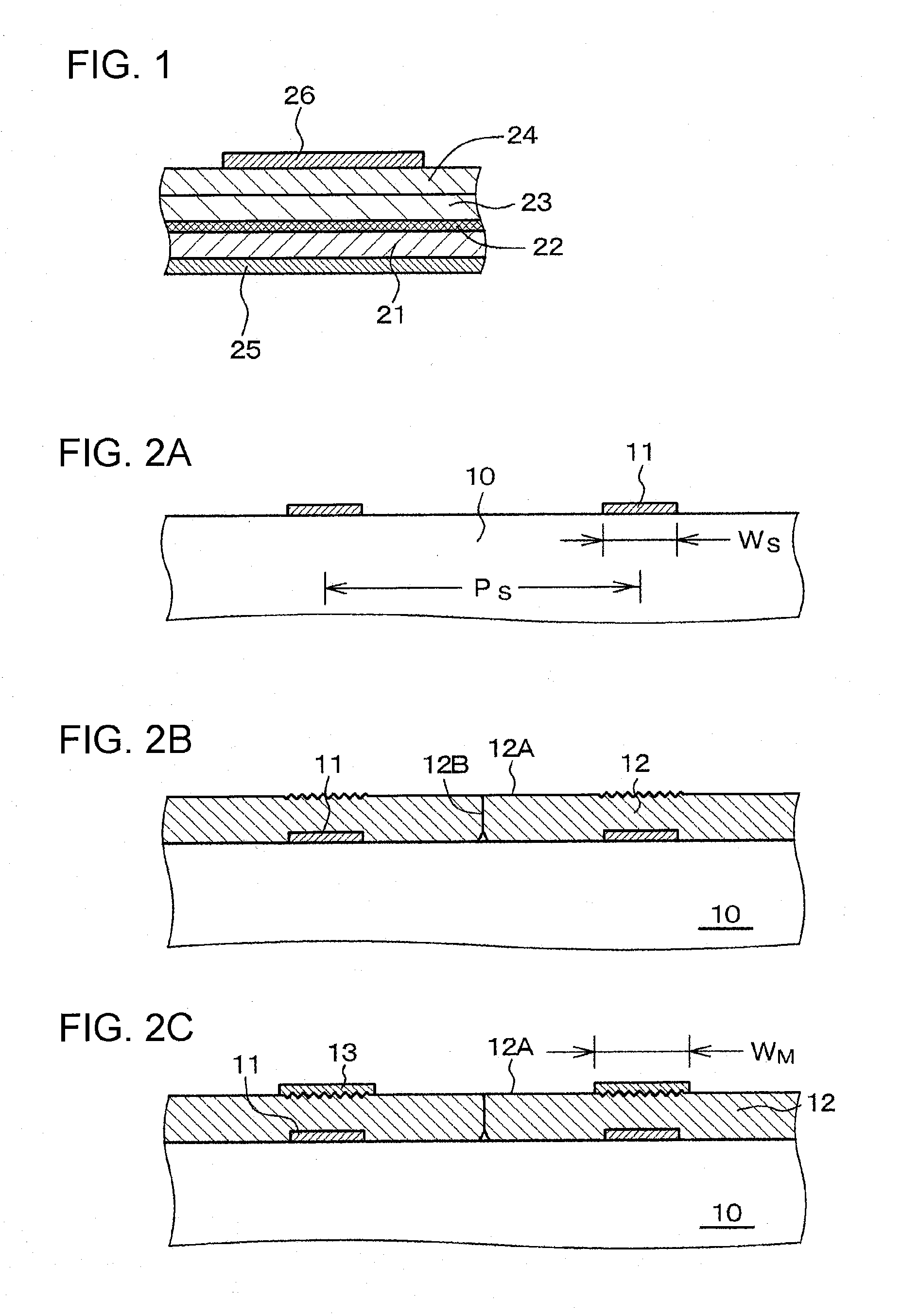
[0094] A first embodiment relates to a GaN-based semiconductor light-emitting element according to a first aspect and a third aspect of the present invention. Furthermore, the first embodiment relates to a method for producing the GaN-based semiconductor light-emitting element according to the first aspect of the present invention. FIG. 1 is a schematic cross-sectional view of the GaN-based semiconductor light-emitting element, more specifically, a light-emitting diode (LED) according to the first embodiment.

[0095] The GaN-based semiconductor light-emitting element according to the first embodiment has a structure in which a first GaN-based compound semiconductor layer 21, an active layer 22, a second GaN-based compound semiconductor layer 23, and a contact layer 24 are stacked. The top face of the first GaN-based compound semiconductor layer 21 is parallel to the a-plane or a nonpolar plane and has a first conductivity type (specifically, n-type). The active layer 22 is disposed o...

second embodiment

[0120] A second embodiment is the modification of the first embodiment.

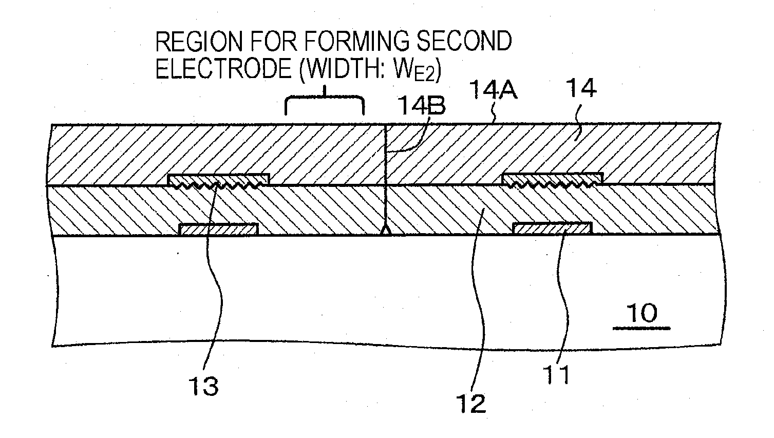
[0121] In the first embodiment, lateral epitaxial growth of the first underlying GaN-based compound semiconductor layers 12 is stopped when opposite side faces 12B of adjacent first underlying GaN-based compound semiconductor layers 12 come into contact with each other. In a GaN compound semiconductor crystal, the coefficient of thermal expansion in the c-axis direction is extremely smaller than the coefficient of thermal expansion of a sapphire substrate. Consequently, the seed layers 11 and the first underlying GaN-based compound semiconductor layers 12 may be detached from the sapphire substrate 10 due to a large change in temperature.

[0122] In second embodiment, in a step similar to [Step-110] in the first embodiment, first underlying GaN-based compound semiconductor layers 12 are formed by lateral epitaxial growth from seed layers 11. The lateral epitaxial growth is stopped before opposite side faces 12B o...

third embodiment

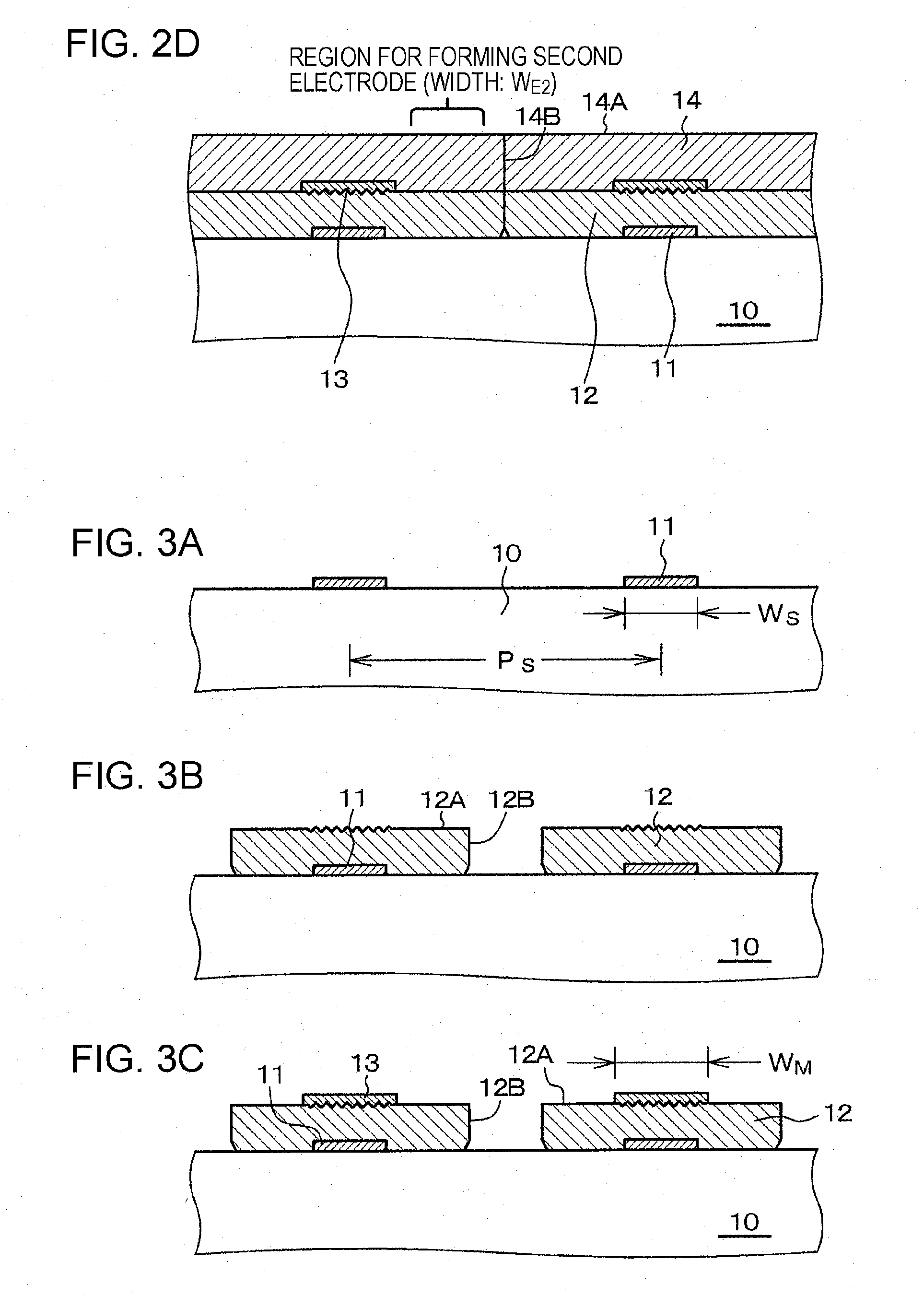
[0137] A third embodiment is the modification of the second embodiment. A main difference between the third embodiment and the second embodiment is the film-forming conditions when the first underlying GaN-based compound semiconductor layers 12 are formed by lateral epitaxial growth from the seed layers 11. In particular, the difference is an increased flow rate of the nitrogen source gas.

[0138] [Step-300]

[0139] The plurality of seed layers 11 that are composed of a GaN-based compound semiconductor and that are apart from each other are formed on the r-plane of a sapphire substrate 10 in the same way as in [Step-100] in the first embodiment. In the third embodiment,

WS=6 μm; and

PS=24 μm.

[0140] [Step-310]

[0141] First underlying GaN-based compound semiconductor layers 12 each having the top face 12A parallel to the m-plane and each having a side face 12B parallel to the c-plane are formed by lateral epitaxial growth from the seed layers 11 in the same way as in [Step-210] in the se...


PUM


Abstract

A GaN-based semiconductor light-emitting element capable of suppressing the occurrence of piezoelectric spontaneous polarization in the thickness direction of an active layer and reducing the driving voltage of a light-emitting diode is provided. The GaN-based semiconductor light-emitting element has a structure with a first GaN-based compound semiconductor layer 21 having the top face parallel to the a-plane and having a first conductivity type, an active layer 22 having the top face parallel to the a-plane, a second GaN-based compound semiconductor layer 23 having the top face parallel to the a-plane and having a second conductivity type, and a contact layer 24 composed of a GaN-based compound semiconductor and having the top face parallel to the a-plane, stacked in that order. The GaN-based semiconductor light-emitting element further includes a first electrode 25 disposed on the first GaN-based compound semiconductor layer 21 and a second electrode 26 disposed on the contact layer 24.

Description

TECHNICAL FIELD [0001] The present invention relates to a GaN-based semiconductor light-emitting element and a method for producing the same. BACKGROUND ART [0002] For example, in the case of blue or green light-emitting diodes (LEDs) each including an n-type GaN layer, an active layer composed of InGaN, and a p-type GaN layer, the layers being stacked, the lattice constant of an InGaN crystal is slightly larger than that of a GaN crystal. Thus, when the n-type GaN layer with the top face parallel to the c-plane, the active layer that is composed of InGaN and in which the top face is parallel to the c-plane, and the p-type GaN layer with the top face parallel to the c-plane are stacked, the active layer is subjected to compression pressure. As a result, piezoelectric spontaneous polarization occurs in the thickness direction of the active layer, causing phenomena such as a shift in the wavelength of light emitted from such a light-emitting diode, an increase in operating voltage, a ...

Claims


Application Information

Patent Timeline
Patent Type & Authority Applications(United States)
IPC IPC(8): H01L33/00H01L21/00H01L33/06H01L33/16H01L33/32
CPCH01L33/007H01L33/16H01L33/14H01L33/0079H01L33/0093
Inventor OKUYAMA, HIROYUKIBIWA, GOSHI
Owner SONY CORP
Why Eureka
Try Eureka