Insulated gate semiconductor device and method for manufacturing the same

a technology of semiconductor devices and gate semiconductors, applied in the direction of semiconductor devices, electrical devices, transistors, etc., to achieve the effect of improving the on characteristics

Active Publication Date: 2008-02-28
MITSUBISHI ELECTRIC CORP
View PDF2 Cites 60 Cited by
  • Summary
  • Abstract
  • Description
  • Claims
  • Application Information

AI Technical Summary

Benefits of technology

[0026]According to the present invention, the ON characteristics can be improved while suppressing the elevation of the for

Problems solved by technology

However, since the N layer 4 is formed between the P base layer 2 and the N− layer 1, holes injected from the collector P la

Method used


Image

  • Insulated gate semiconductor device and method for manufacturing the same
  • Insulated gate semiconductor device and method for manufacturing the same
  • Insulated gate semiconductor device and method for manufacturing the same

Examples


first embodiment

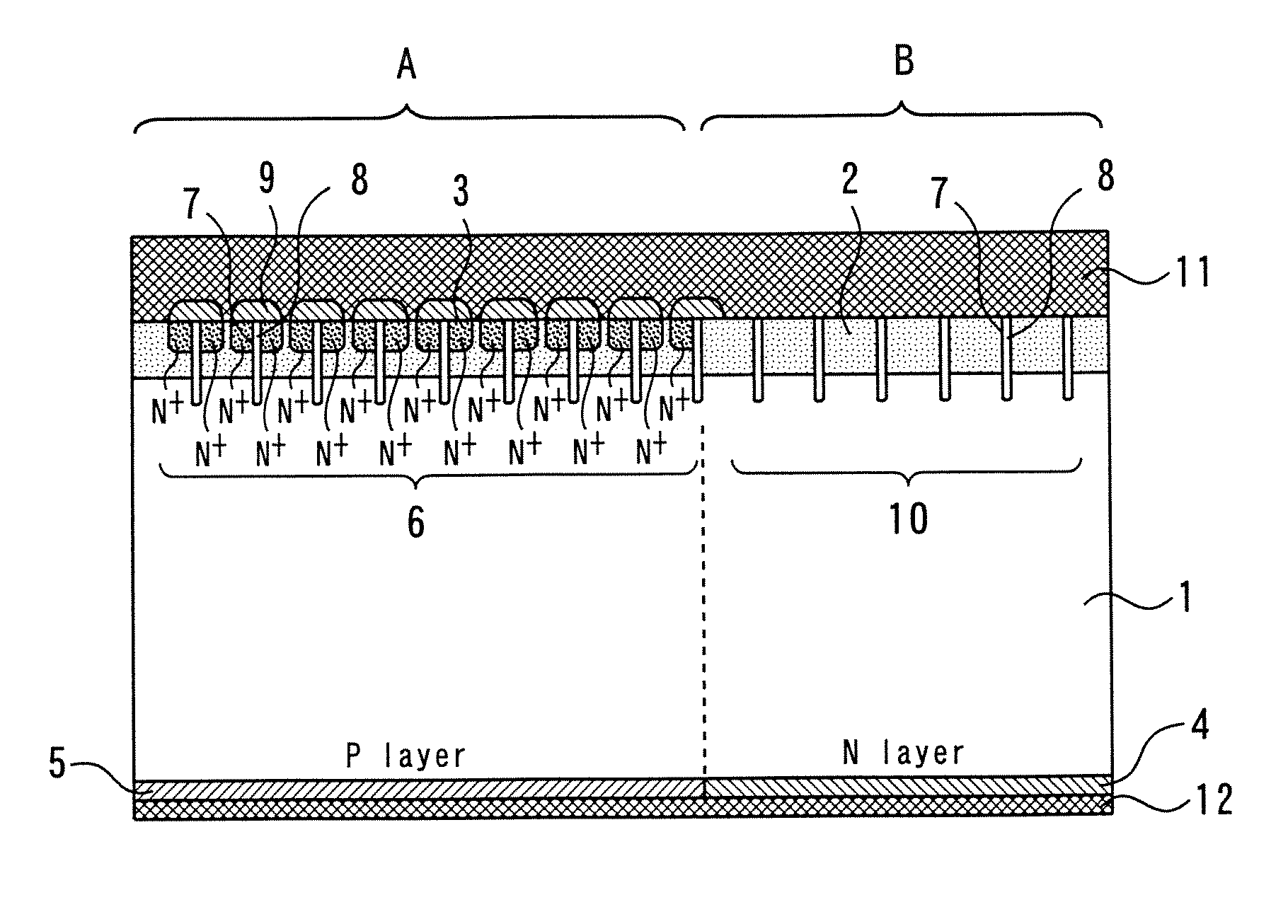
[0051]FIG. 1 is a sectional view of an insulated gate semiconductor device according to the first embodiment of the present invention. The semiconductor device is formed using an N− substrate 1 containing an n-type impurity, and the N− substrate 1 has a first major surface (upper major surface) and a second major surface (lower major surface). The N− substrate 1 has at least one region A (first region), and a region B (second region) is provided so as adjoin thereto. Emitter layers 3 are provided in the region A, but no emitter layers 3 are provided in the region B.

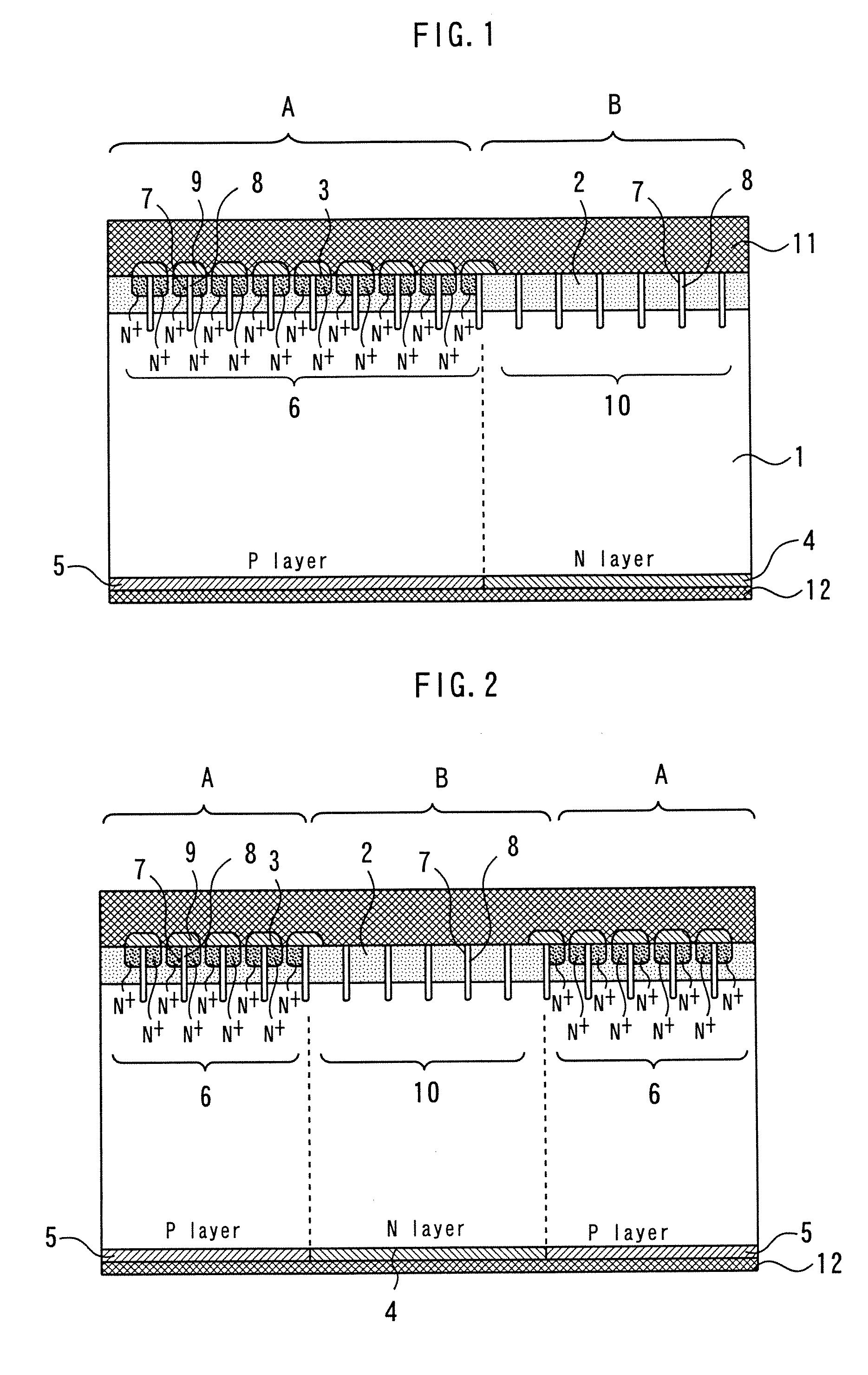
[0052]In the region A and the region B, a P base layer 2 wherein a p-type impurity is diffused is selectively provided in the vicinity of the first major surface side of the N− substrate 1. In the region A, a plurality of first trenches 6 are provided at intervals of about 2 to 10 μm so as to penetrate the P base layer 2 from the first major surface side of the N− substrate 1. (As FIG. 2 shows, when a plurality of regions...

second embodiment

[0078]An insulated gate semiconductor device according to the second embodiment will be described referring to FIG. 9. Here, the description will center on the aspects different from the aspects in the first embodiment.

[0079]As FIG. 9 shows, a carrier accumulating layer 13 is formed so as to contact the P base layer 2 on the second major surface side of the P base layer 2 of the N− substrate 1, as a fifth semiconductor layer containing an n-type impurity. The concentration of the n-type impurity in the carrier accumulating layer 13 is higher than the impurity concentration of the N− substrate 1. Other configurations are identical to the configurations of the first embodiment.

[0080]Next, the operation of the insulated gate semiconductor device shown in FIG. 9 will be described. The operation of the IGBT shown in FIG. 9 is basically the same as the operation of the IGBT shown in FIG. 1. In the case of the IGBT operation shown in FIG. 9, the carrier accumulating layer 13 acts as the ba...

third embodiment

[0085]An insulated gate semiconductor device according to the third embodiment will be described referring to FIG. 10. Here, the description will center on the aspects different from the aspects in the first and second embodiments.

[0086]In the insulated gate semiconductor device shown in FIG. 10, the impurity concentration of the P base layer 2 provided in the region A is different from the impurity concentration of the P base layer 2b provided in the region B. Specifically, the impurity concentration of the P base layer 2b provided in the region B is lower than the impurity concentration of the P base layer 2 provided in the region A. Other configurations are identical to the configurations of the first embodiment.

[0087]The operation of the IGBT shown in FIG. 10 is basically the same as the operation of the IGBT shown in FIG. 1. In the third embodiment, the first semiconductor layer functioning as the P base layer of the IGBT has a different impurity concentration from the impurity...


PUM


Abstract

There is provided a structure wherein an emitter layer 3 is provided in the region A on the first major surface side of a semiconductor substrate 1, and emitter layer 3 is not provided in the region b. There is provided a structure wherein a collector P layer 5 is provided in the region A on the second major surface side of a semiconductor substrate 1, and a cathode N layer 4 is provided in the region B. Specifically, there is provided a structure wherein IGBTs are composed in the region A, and diodes are composed in the region B. By the above-described structure, ON characteristics when the gate is turned on can be improved while suppressing the elevation of the forward voltage Vf and the recovery current of the diodes.

Description

BACKGROUND OF THE INVENTION[0001]1. Field of the Invention[0002]The present invention relates to an insulated gate semiconductor device and a method for manufacturing the same, and more specifically to an insulated gate bipolar transistor having a built-in diode and a method for manufacturing the same.[0003]2. Background Art[0004]In power electronics for driving motors or the like, an insulated gate bipolar transistor (IGBT) is used as a switching element in the region wherein the rated voltage is 300 V or higher. Normally, a reflux diode is connected to the IGBT in parallel.[0005]FIG. 35 shows the cross-sectional structure of a conventional IGBT. An N+ buffer layer 112 is formed on a collector P layer 5, and an N− layer 1 is formed thereon. On the surface of the N− layer 1, a P base layer 2 wherein a p-type impurity is diffused is selectively formed. On the surface of the P base layer 2, an emitter layer 3 wherein an n-type impurity of a high concentration is selectively diffused i...

Claims


Application Information

Patent Timeline
IPC IPC(8): H01L27/082H01L21/336H01L29/739H01L29/78
CPCH01L29/0839H01L29/4236H01L29/861H01L29/7391H01L29/7397H01L29/66348H01L29/70
Inventor TAKAHASHI, HIDEKI
Owner MITSUBISHI ELECTRIC CORP
Why Eureka
Try Eureka