Display device, driving method thereof, and electronic apparatus

a display device and driving method technology, applied in static indicating devices, instruments, electroluminescent light sources, etc., can solve the problems of affecting the high precision display, pixel circuits are not suitable for high precision displays, and complicated pixel circuits, so as to reduce the number of constituent elements, reduce the number of layout areas, and improve the effect of display

Active Publication Date: 2008-02-28
JOLED INC
View PDF21 Cites 32 Cited by
  • Summary
  • Abstract
  • Description
  • Claims
  • Application Information

AI Technical Summary

Benefits of technology

[0013]Preferably, the power supply scanner adjusts the first timing when the power supply line is dropped from the first potential to the second potential to allow a light emission period of the light emitting element to be adjusted. The main scanner may remove the application of the control signal to the scan line at a fifth timing after the fourth timing to make the sampling transistor non-conductive, while the signal selector may change the signal line from the reference potential at a fourth timing after the sampling transistor becomes conductive, and a period between the fourth timing and the fifth timing may be set properly. Consequently, a correction of a mobility of the driver transistor may be added to the signal potential when the signal potential is held in the holding capacitor. Furthermore, the main scanner may remove the application of the control signal to the scan line at the fifth timing when the signal potential is held in the holding capacitor to make the sampling transistor enter a non-conductive state to electrically disconnect the gate of the driver transistor from the signal line, thereby making a gate potential of the driver transistor follow a variation in a source potential and maintain a gate-source voltage constant.
[0014]According to an embodiment of the present invention, in an active matrix type display device using light emitting elements, such as organic EL devices, as pixels, each pixel has a threshold value correction function of the driver transistor. Preferably, each pixel also has a mobility correction function, a secular variation correction function (bootstrap operation) of an organic EL device and other functions. A current-technology pixel circuit having the correction functions of this type has a large layout area because of a number of constituent elements, so that the pixel circuit is not suitable for a high precision display. According to an embodiment of the present invention, switching pulses are used as a power supply voltage to be supplied to each pixel, thereby reducing the number of constituent elements. By using switching pulses as the power supply voltage, a switching transistor for threshold voltage correction and a scan line for scanning the gate of the switching transistor may become unnecessary. Accordingly, constituent elements of the pixel circuit and wirings can be reduced considerably and a pixel area can be reduced to realize a high precision display.
[0015]In order to correct a threshold voltage of a driver transistor, the gate and source potentials of the driver transistor are reset in advance. According to an embodiment of the present invention, by adjusting the timings when the source and gate potentials of the driver transistor are reset, a threshold voltage correction operation can be executed reliably. More specifically, when the gate potential of the driver transistor is reset to the reference potential and the source potential is set to the second potential (low level of a power supply potential), the power supply line is dropped beforehand to the second potential. In this manner, the threshold voltage correction operation can be executed reliably without being affected by the wiring capacitance and the resistance. As has been described, the display device of an embodiment of the present invention operates without being affected by the wiring capacitance of the pixel circuit so that the embodiment can be applied to a high precision and large screen display device.

Problems solved by technology

However, current-technology active matrix type, flat panel emissive display devices have a variation in threshold voltages and mobilities of transistors for driving light emitting elements due to process variations.
However, the proposed pixel circuit provided with the correction function requires a wiring for supplying an electrical potential for correction, switching transistors, and switching pulses, resulting in a complicated pixel circuit.
Since there are many constituent elements of a pixel circuit, these elements hinder a high precision display.
A current-technology pixel circuit having the correction functions of this type has a large layout area because of a number of constituent elements, so that the pixel circuit is not suitable for a high precision display.

Method used


Image

  • Display device, driving method thereof, and electronic apparatus
  • Display device, driving method thereof, and electronic apparatus
  • Display device, driving method thereof, and electronic apparatus

Examples


Embodiment Construction

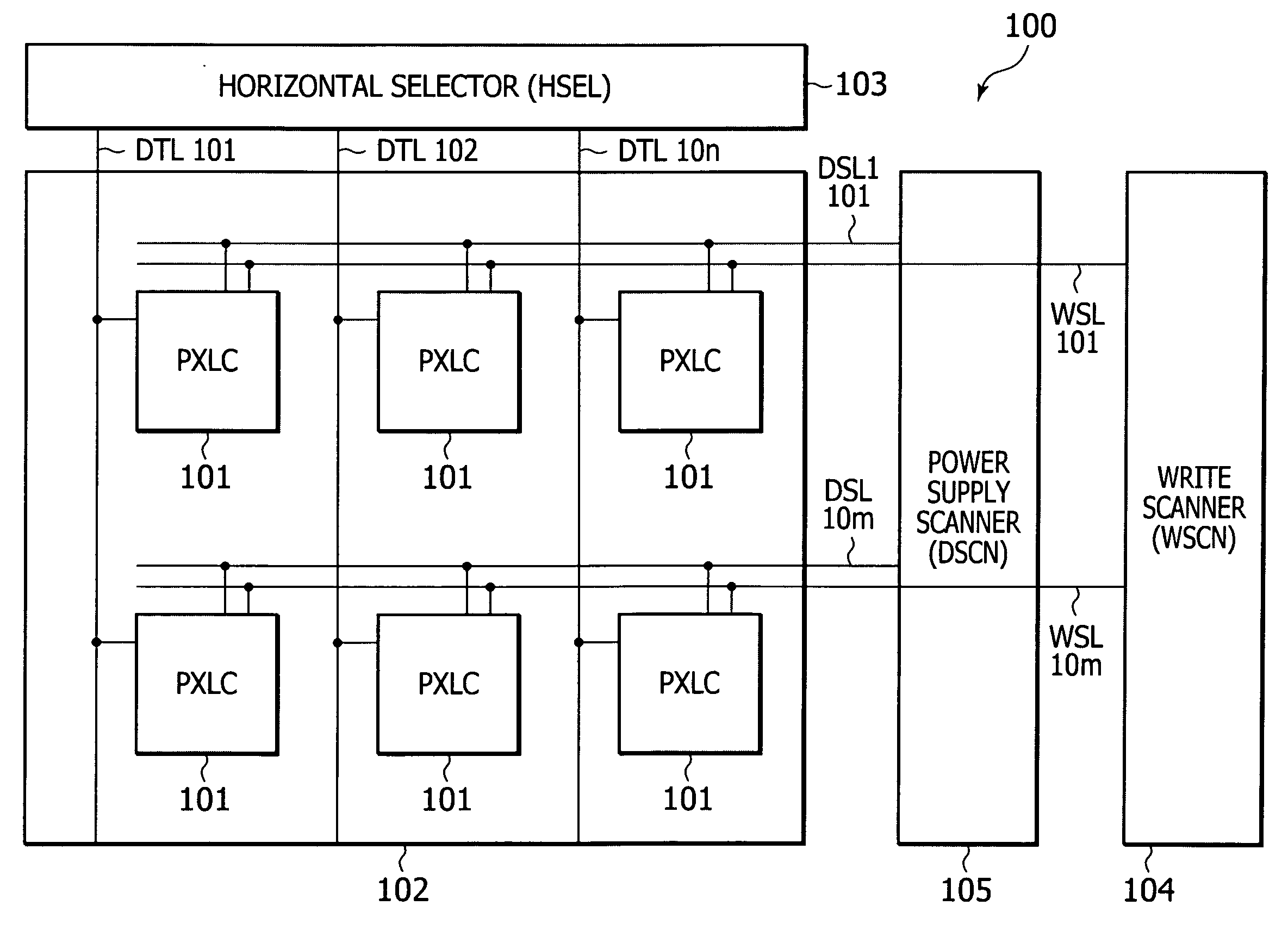
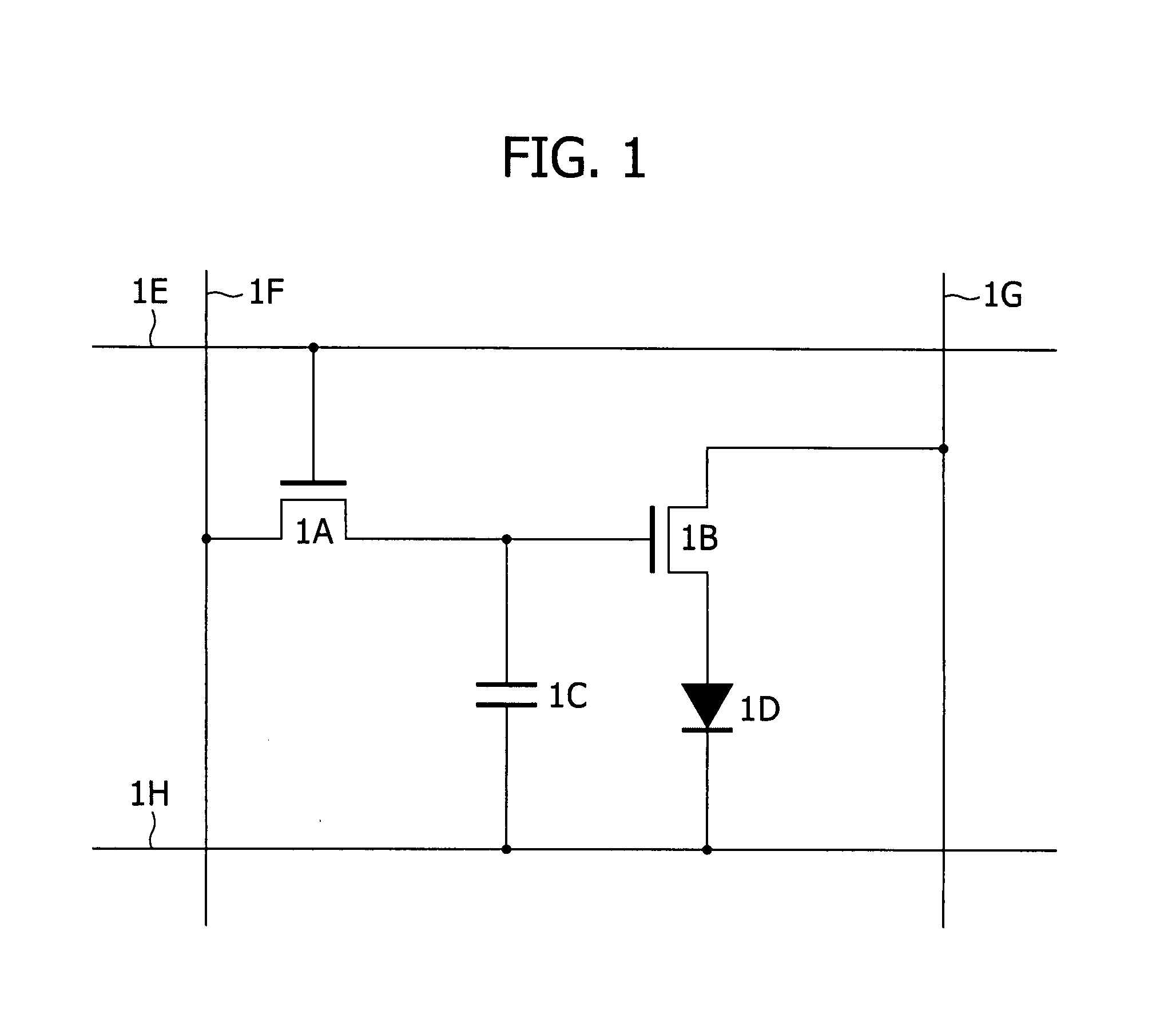
[0049]Embodiments of the present invention now will be described in detail with reference to the accompanying drawings. First, in order to make it easy to understand an embodiment of the present invention and clarify the background, the general structure of a display device will be described briefly with reference to FIG. 1. FIG. 1 is a schematic circuit diagram showing one pixel of a general display device. As shown in FIG. 1, this pixel circuit has a sampling transistor 1A disposed at a cross point of a scan line 1E and a signal line 1F disposed orthogonally. The sampling transistor 1A is an n-type. The gate of the transistor 1A is connected to the scan line IE and the drain of the transistor 1A is connected to the signal line 1F. One electrode of a holding capacitor IC and a gate of a driver transistor 1B are connected to the source of the sampling transistor 1A. The driver transistor 1B is an n-type. The drain of the driver transistor 1B is connected to a power supply line 1G an...


PUM


Abstract

A display device includes a pixel array unit and a driver unit. A sampling transistor samples a signal potential to hold the signal potential in a holding capacitor. A driver transistor flows a drive current to a light emitting element in accordance with the signal potential held. A power supply scanner in the driver unit changes a power supply line from a first potential to a second potential before the sampling transistor samples the signal potential. A main scanner in the driver unit makes the sampling transistor conductive to apply a reference potential from the signal line to the gate of the driver transistor and to set the source of the driver transistor to a second potential. The power supply scanner changes the power supply line from the second potential to the first potential to hold a voltage corresponding to a threshold voltage off the driver transistor in the holding capacitor.

Description

BACKGROUND OF THE INVENTION[0001]1. Field of the Invention[0002]The present invention relates to an active matrix type display device using light emitting elements as pixels and a driving method thereof. The present invention relates also to an electronic apparatus in which this type of display device is assembled.[0003]2. Description of Related Art[0004]The development of emissive, flat panel display devices using an organic electroluminescent (EL) device as an optical emitting element has been made vigorously in recent years. An organic EL device is a device utilizing a phenomenon in which as an electric field is applied to an organic thin film, light emission occurs. Since the organic EL device is driven by an application voltage of 10 V or lower, the device consumes a low power. Since the organic EL device is an emissive device which emits light by itself, no illumination member is required and the device can be made light in weight and thin easily. Furthermore, a response time ...

Claims


Application Information

Patent Timeline
Patent Type & Authority Applications(United States)
IPC IPC(8): G06F3/038H05B44/00
CPCG09G3/3266G09G3/3258G09G2320/043G09G2300/0819
Inventor IIDA, YUKIHITOUCHINO, KATSUHIDE
Owner JOLED INC
Why Eureka
Try Eureka