Single ic-chip design on wafer with an embedded sensor utilizing RF capabilities to enable real-time data transmission

a technology of embedded sensors and ic-chips, applied in semiconductor/solid-state device testing/measurement, electric signalling details, instruments, etc., can solve problems such as inability to provide real-time data feedback from monitors or product wafers, affecting the accuracy of probes, and available devices such as temp probes that require timely setups, so as to improve chamber and chuck temperature accuracy. , the effect of improving the accuracy of the temperatur

Inactive Publication Date: 2008-02-28
GLOBALFOUNDRIES INC
View PDF14 Cites 9 Cited by
  • Summary
  • Abstract
  • Description
  • Claims
  • Application Information

AI Technical Summary

Benefits of technology

[0010] It is a further object of the present invention to provide an apparatus and method that provides feedback data relating to process conditions, e.g., temperature, to processing tool controllers to use for real-time control of the chamber's critical temperature environment especially at the wafer surface. By having a fully populated monitor wafer with built-in temperature sensors able to communicate real-time, there is provided concurrent tool recipe development that greatly improves both chamber and chuck temperature accuracy.
[0011] It is yet a further object of the present invention to provide a system and method for fabricating a wafer that senses and communicates, via a wireless communications transmission, actual chamber operating conditions as seen by a typical process wafer. Parameters such as temperature, RF power, gas flows, pressures, DC bias voltages are observed and recorded for chamber to chamber matching. Such a monitor wafer could easily be moved from chamber to chamber and / or tool to tool to serve as a common calibration standard device.

Problems solved by technology

These do not provide real-time data feedback from monitor or product wafers that accurately reflect the process conditions as seen by the Si wafer within a process tool during operation or that can directly control the process tool.
Available devices such as temp probes require timely setups and probe accuracy is questionable.
Thermocouple wafers require wires leading from a wafer that are cumbersome and must have built-in feed-throughs to make connections to external recording devices.
Thermocouples are bonded to the wafer surface, and use of temperature dots typically attached to the wafer surface display a color variant requiring visual distinction yielding lower accuracy and not applicable to product or to feedback information for tool adjustment.
These methods are intrusive, time consuming, and not representative of actual wafer conditions, and are typically one time use applications.

Method used


Image

  • Single ic-chip design on wafer with an embedded sensor utilizing RF capabilities to enable real-time data transmission
  • Single ic-chip design on wafer with an embedded sensor utilizing RF capabilities to enable real-time data transmission

Examples


Embodiment Construction

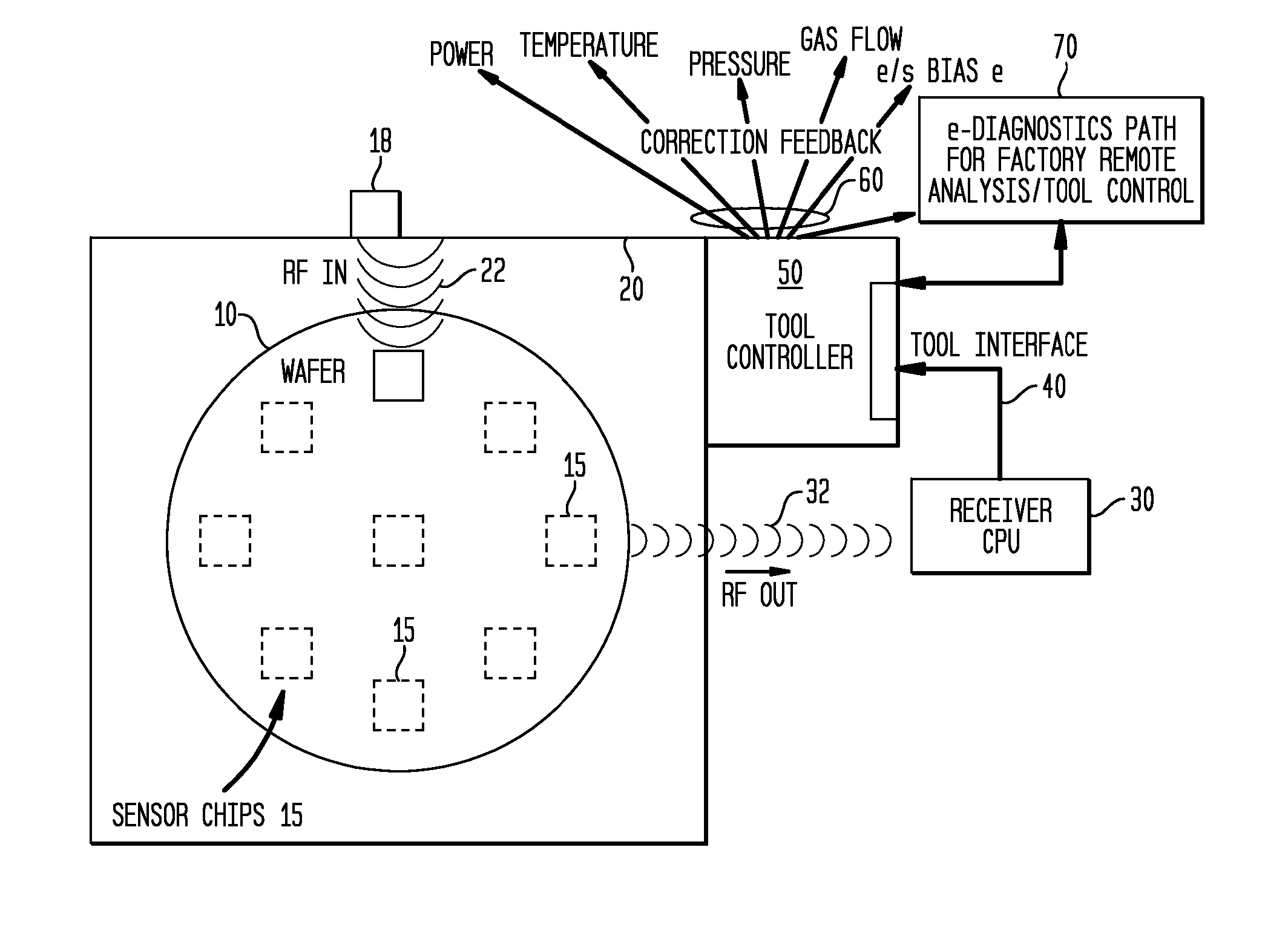
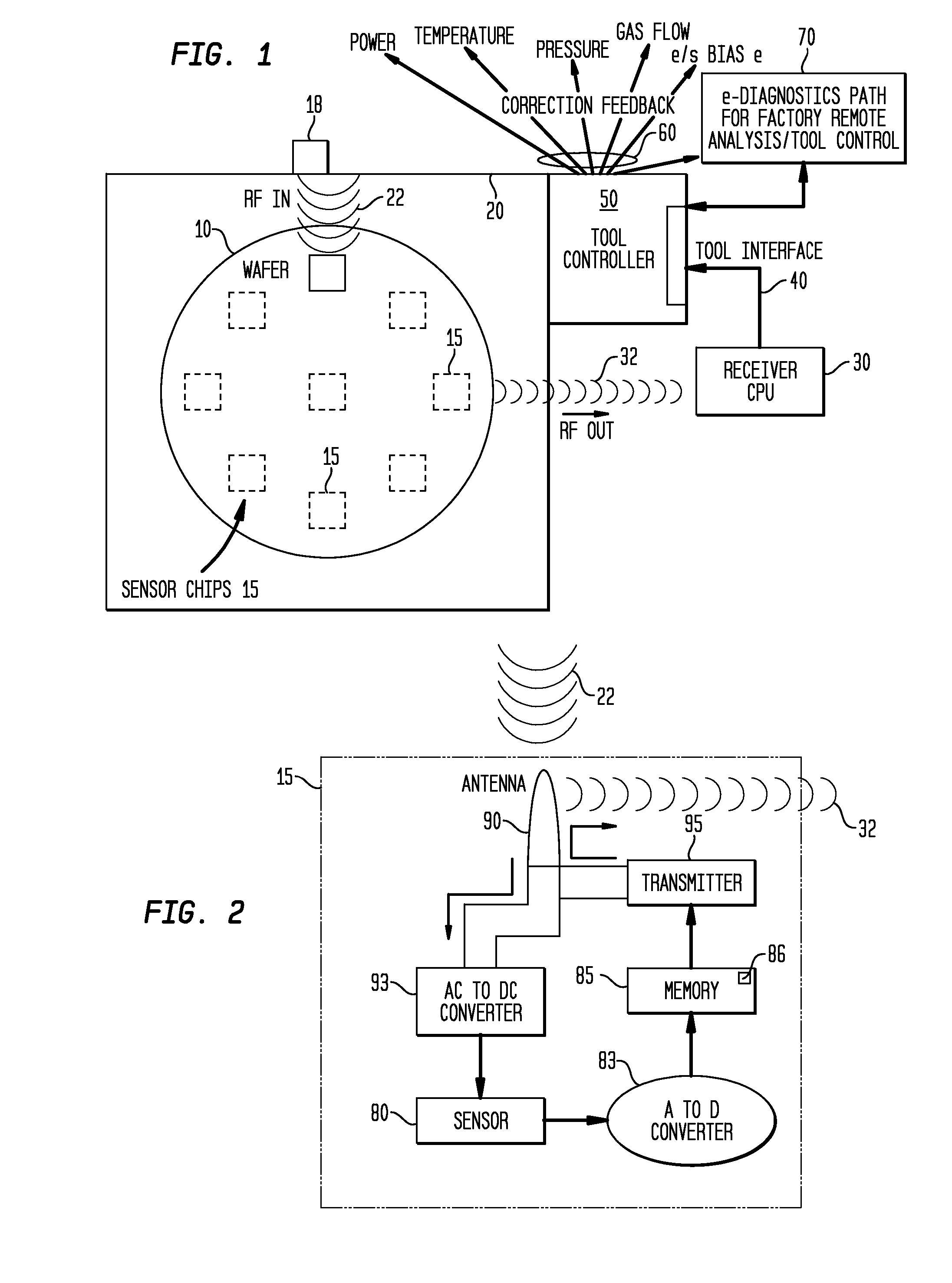
[0017] With reference to the accompanying drawings, FIG. 1 illustrates a schematic diagram of a single semiconductor (e.g., silicon) monitor wafer 10 packaged with an array of embedded IC chips designed with wireless communications capabilities. The monitor wafer is populated with a plurality of individual sensor device circuit chips 15 that utilize RF wireless transmission to communicate with an external RF communications receiver 30. As will be described, each chip has a unique identification (chip ID) associated therewith such that RF signals and process condition data received from a particular sensor device will be automatically identified and associated with that sensor. It is understood that while the exemplary embodiment described herein is directed to sensing of temperature by providing temperature sensor devices 15, it is understood that the apparatus is equally adapted to sense other process conditions such as, e.g., power, pressure, gas flow, e / s bias, etc. via suitable ...


PUM


Abstract

An apparatus and method for real-time monitoring process conditions of a semiconductor wafer processing operation. A semiconductor wafer subject to processing in a wafer processing tool is embedded with one or more sensor devices. In response to receipt of wireless electromagnetic signals, the embedded sensor devices are activated for generating sensory data. The electromagnetic signals are further utilized to activate a transmitter device provided in the wafer to wirelessly transmit the sensory data generated from the activated embedded sensor device. The transmitted electromagnetic signals comprising the sensory data are communicated to a control device for controlling processing conditions of the process tool based upon the received sensory data.

Description

RELATED APPLICATIONS [0001] This application is a divisional of U.S. application Ser. No. 10 / 907,798, filed Apr. 15, 2005.BACKGROUND OF THE INVENTION [0002] 1. Field of the Invention [0003] The present invention relates generally to semiconductor wafer fabrication and particularly, to an improved system and method for manufacturing semiconductor chips using real-time process condition data feedback. [0004] 2. Description of the Prior Art [0005] In current semiconductor wafer fabrication processes and systems, there is no ‘real-time’ data feedback from monitor or product wafers that accurately reflects the process conditions to the wafer within a process tool during operation. Current methods used in monitoring process chamber parameters (e.g., temp, chuck e / s bias / heat zones, pressure, gas flows, plasmas) of most tools are in situ sensors remotely placed within the chamber. These do not provide real-time data feedback from monitor or product wafers that accurately reflect the proces...

Claims


Application Information

Patent Timeline
Patent Type & Authority Applications(United States)
IPC IPC(8): H01L21/00G08B1/08
CPCH01L21/67294
Inventor GLUSCHENKOV, OLEGLITTLE, TIMOTHY E.SNYDER, GARY L.
Owner GLOBALFOUNDRIES INC
Why Eureka
Try Eureka