Thin film transistor array substrate and manufacturing method thereof

a technology of thin film transistors and array substrates, which is applied in the direction of instruments, semiconductor devices, electrical apparatuses, etc., can solve the problems of panel scrapping, difficult to control a good taper angle,

Inactive Publication Date: 2008-03-06
CHUNGHWA PICTURE TUBES LTD
View PDF3 Cites 5 Cited by
  • Summary
  • Abstract
  • Description
  • Claims
  • Application Information

AI Technical Summary

Benefits of technology

[0006]In order to solve the mentioned problem, one object of the present invention is to provide a thin film transistor array substrate and the manufacturing method thereof. It utilizes a patterned thin film disposed at the cross portion of the source lines and the Cs lines and between two layers so as to solve the short problem at the cross portion.

Problems solved by technology

Due to the fact that the complex metal is used, it is difficult to control a good profile of the taper angle because of the etching rate of different materials so as to easily cause the undercut effect.
This defect will cause the light line of the liquid crystal display device while turning on the panel and this panel must perform the array test to find the defect and perform the laser repair.
Further, the panel is scrapping.

Method used


Image

  • Thin film transistor array substrate and manufacturing method thereof
  • Thin film transistor array substrate and manufacturing method thereof
  • Thin film transistor array substrate and manufacturing method thereof

Examples


Embodiment Construction

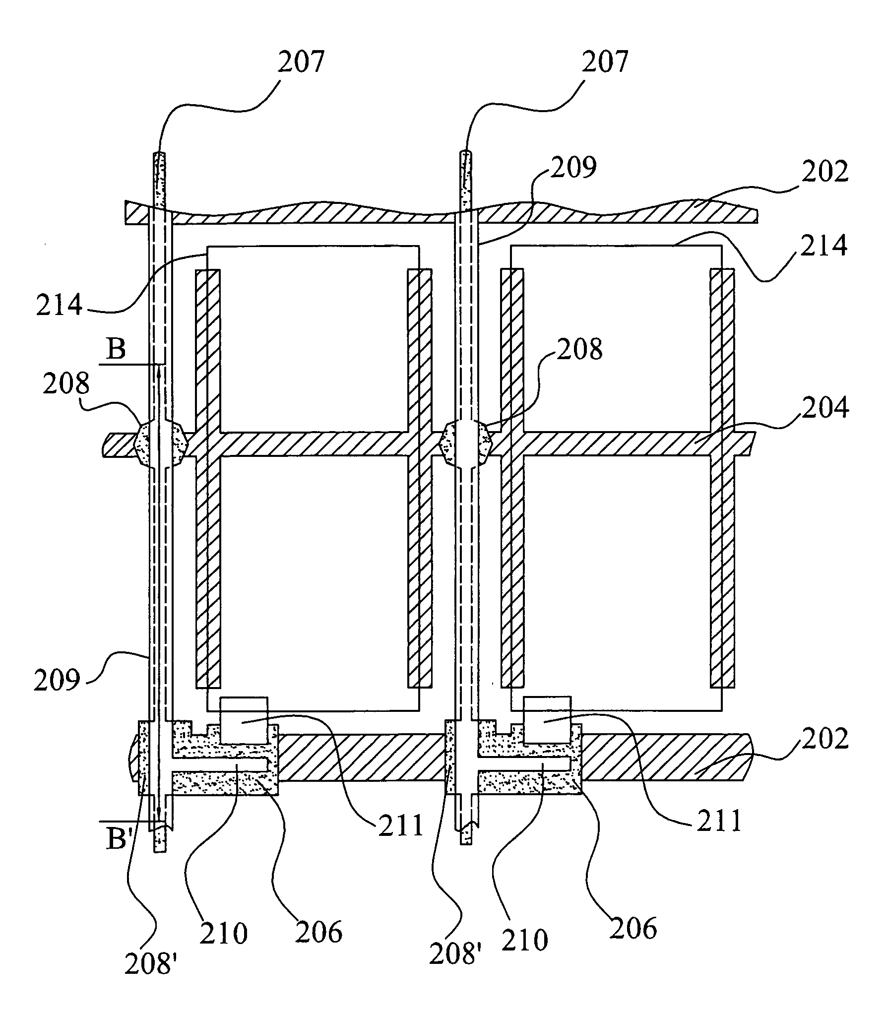
[0018]FIG. 3 is a plan view of the thin film transistor array substrate illustrated one embodiment of the present invention. Such as shown in FIG. 3, in the present embodiment, a thin film transistor (TFT) array substrate includes a plurality of scan lines 202 and a plurality of source lines 209 disposed on the substrate and define a plurality of pixel regions. A plurality of storage capacitance lines (Cs line) 204 are disposed on the substrate in a direction extending along to across the pixel regions, and each of Cs lines 204 is essentially perpendicular to each of the source lines 209 to form a cross portion. A plurality of patterned thin films 208 are disposed on Cs lines 204 and above the cross portion.

[0019]Following the foregoing, in the present embodiment, the scan lines 202 and the Cs lines 204 are simultaneously formed in the same process. After, an insulating layer (not shown FIG. 3) is disposed to cover the scan lines 202 and the Cs lines 204. Wherein, the patterned thin...


PUM


Abstract

A thin film transistor array substrate and the manufacturing method thereof are disclosed herein. A first patterned metal layer, an insulating layer, a patterned layer, and a second patterned metal layer are sequentially formed on a substrate. Then, a plurality of scan lines and a plurality of source lines are disposed on the substrate and define a plurality of pixel regions. A plurality of the storage capacitance lines are disposed on the substrate in a direction extending along the scan lines and across the pixel regions, wherein each of the storage capacitance lines is essentially perpendicular to each of the source lines and to form a cross portion. A plurality of patterned thin films are disposed on the storage capacitance lines and above the cross portion.

Description

BACKGROUND OF THE INVENTION[0001]1. Field of the Invention[0002]The present invention generally relates to a liquid crystal display device, and more particularly relates to a thin film transistor (TFT) array substrate for the liquid crystal display device and the manufacturing method thereof.[0003]2. Description of the Prior Art[0004]FIG. 1 is illustrated a plan view of the liquid crystal display according to the prior art. Referring to FIG. 1, scan lines 102 and source lines 109 are disposed to cross to define a plurality of pixel regions. The storage capacitance line (Cs line) 104 is extended over the pixel region to cross the source line 109. An ohmic contact thin film 106, a source electrode 110 and a drain electrode 111 are disposed on the scan line 102. Besides, a pixel electrode 114 is disposed in the pixel region. Wherein, scan lines 102 and the Cs lines 104 are simultaneously formed and there is an insulating layer, not shown in the figure, covered thereon. The Cs line 104 ...

Claims


Application Information

Patent Timeline
Patent Type & Authority Applications(United States)
IPC IPC(8): H01L29/04
CPCG02F1/1345G02F1/136213H01L27/1244H01L27/1255H01L27/124G02F2201/50
Inventor HUANG, JUN-YAOFU, KUANG-CHENGLIN, JEN-CHIEHYEH, CHIN-LUNG
Owner CHUNGHWA PICTURE TUBES LTD
Why Eureka
Try Eureka