Processing with Reduced Line End Shortening Ratio

Active Publication Date: 2008-03-06
TAIWAN SEMICON MFG CO LTD +1
View PDF14 Cites 0 Cited by
  • Summary
  • Abstract
  • Description
  • Claims
  • Application Information

AI Technical Summary

Benefits of technology

[0005]The present invention relates to a process for forming device features with reduced line end shortening (LES). In accordance with one aspect of the invention, a method for reducing LES includes providing a substrate prepared with a device layer or layers of a gate conductor formed thereon with a patterned resist layer disposed above the device layer or layers of the gate conductor. The method further comprises partially trimming the resist layer to produce resist dimensions less than desired dimensions and patterning the device layer or layers of the gate conductor using the partially trimmed

Problems solved by technology

However, conventional resist trimming processes cause the polysilicon line end to pull back much more than do its sides.
However, such a high LES ratio is not tolerable for some devices, such as SRAM ICs, particularly in light of shrinking device dimensions coupled with increased density.
This results in current leakage, as represented by the dotted line in FIG. 1, between the transistors.
Hard mask processes, however, besides contributing to higher costs a

Method used


Image

  • Processing with Reduced Line End Shortening Ratio
  • Processing with Reduced Line End Shortening Ratio
  • Processing with Reduced Line End Shortening Ratio

Examples


Embodiment Construction

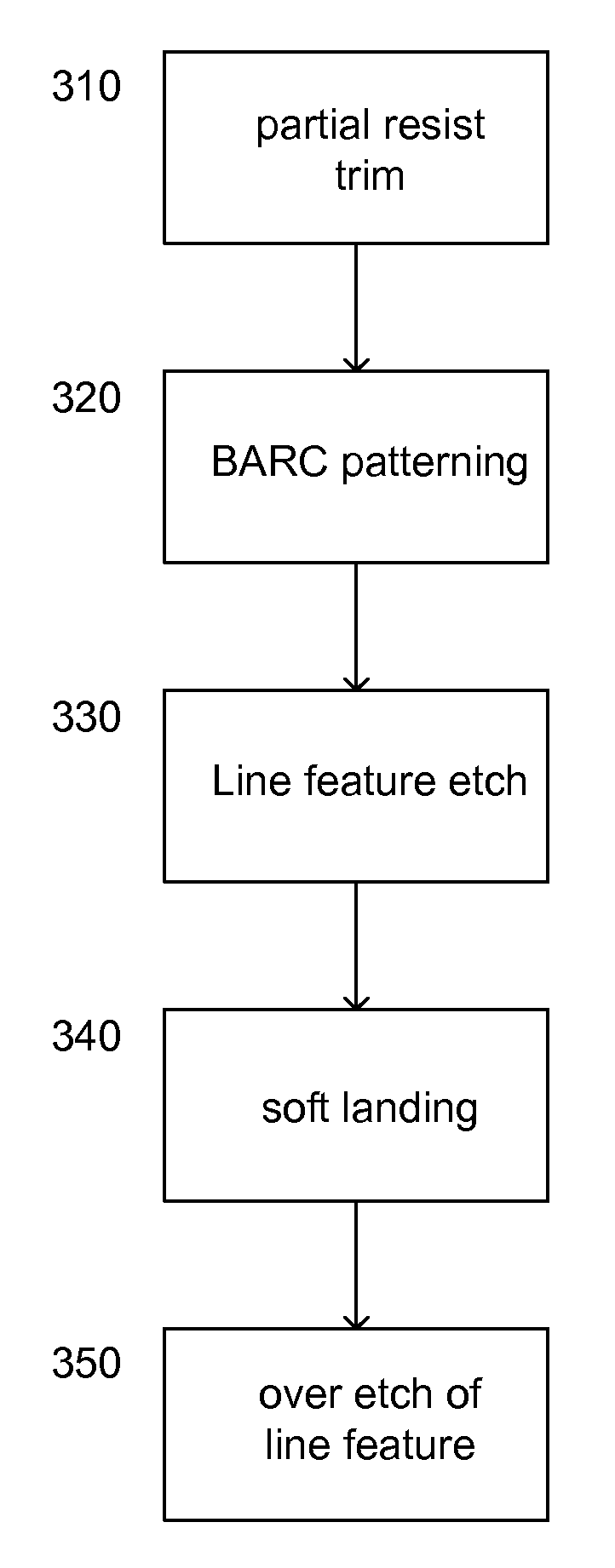
[0010]The present invention relates to semiconductor processing. More particularly, the present invention provides a process for forming patterned line features with reduced line end shortening. In one embodiment, the line feature comprises polysilicon lines which serve, for example, as gate conductors. Forming other types of line features is also contemplated and within the scope of the invention, particularly where low LES ratio is desirable.

[0011]In accordance with one embodiment of the invention, forming a line feature with sub-ground rule dimensions can be achieved as part of the etch that forms the line feature. The etch can include an initial etch with appropriate etch chemistry which substantially produces the feature based on a patterned resist mask and an over-etch to complete the patterning of the feature, wherein the initial etch uses an appropriate etch chemistry to trim the line feature to desired dimensions. By trimming the line feature as part of the etch that forms ...


PUM


Abstract

A method for forming device features with reduced line end shortening (LES) includes trimming the device feature to achieve the desired sub-ground rule critical dimension during the etch to form the device feature.

Description

FIELD OF THE INVENTION[0001]The present invention relates generally to semiconductor processing, and more particularly to a method for forming device features with reduced line end shortening (LES).BACKGROUND OF THE INVENTION[0002]To achieve feature sizes that are smaller than the lithographic ground rule, a process known as resist trimming is used. For example, to achieve transistor gate length smaller than ground rule, the patterned resist mask can be trimmed to reduce the critical dimension (CD) of the polysilicon line to the target dimension. However, conventional resist trimming processes cause the polysilicon line end to pull back much more than do its sides.[0003]The distance by which the photoresist line ends is shortened as compared to the reduction in line width is referred to as the line end shortening (LES) ratio. The LES ratio is typically >1.5 to 2. However, such a high LES ratio is not tolerable for some devices, such as SRAM ICs, particularly in light of shrinking...

Claims


Application Information

Patent Timeline
IPC IPC(8): H01L23/48H01L21/311
CPCH01L21/32137H01L21/32139
Inventor CONG, HAILOH, WEI LOONGGOPAL, KRISHANZHANG, XINZHOU, MEI SHENGYELEHANKA, PRADEEP RAMACHANDRAMURTHY
Owner TAIWAN SEMICON MFG CO LTD
Why Eureka
Try Eureka