Method and system for measuring patterned structures

a pattern structure and measurement method technology, applied in the field of measuring techniques, can solve the problems of insufficient consideration of methods, unfavorable treatment effect, and ineffectiveness, and achieve the effects of high accuracy, good chance of obtaining accurate results, and confidence in results

Inactive Publication Date: 2008-03-06
NOVA MEASURING INSTR LTD
View PDF21 Cites 22 Cited by
  • Summary
  • Abstract
  • Description
  • Claims
  • Application Information

AI Technical Summary

Benefits of technology

[0029] According to the present invention, at least one parameter of the profile considered in an optical model used for measurements is determined by analyzing at least one preliminary measurement applied to a predetermined site on the structure (wafer). The preliminary measurement is inherently different from further measurements by either the type of site under measurements or the measurement conditions (angle, polarization, wavelength range, diffraction order, etc.). For example, the preliminary measurement utilizes normal incidence of an illuminating beam, while the further measurement utilizes oblique illumination. Data (parameters) obtained through this preliminary measurement is used for optimizing the fitting procedure, thereby improving further measurements applied to other locations on the structure.
[0039] The scatterometry based measurement technique provides the collection of a large amount of data from each measured profile, e.g., the diffraction efficiency in a large number of different angles or a large number of wavelengths. This richness of data may allow the fitting of the measurements to the results of a multi-parameter model describing the measured profile, thus providing more information than merely stating the CD. This additional information also provides confidence in the results, particularly if the effective number of independent measured values is significantly larger than the number of free parameters in the model. Since exact models describing diffraction from general profiles and in general situations have been developed for years and are known to be of high accuracy, these methods have a good chance of obtaining accurate results.
[0040] The system according to the invention can be applied as an integrated metrology tool. In contrast to all conventionally used off-line measurement tools, occupying a large footprint and requiring additional manual operations that slow down the entire fabrication process and allow only the measurement of samples from each production lot, the system of the present invention may be integrated as part of the production machine, thus allowing full automation of the manufacturing process. For this integration to be possible, the system should be very economical in space.
[0041] Additionally, the operation of the system is fast enough, so that every semiconductor wafer in the production line can be measured, allowing closer control over the process. The system of the present invention enables a multi-stage measurement procedure, thereby improving the quality of the entire measurement. The measurement technique according to the invention requires only a small measurement site in accordance with the area constraints, which characterize current lithography.

Problems solved by technology

However, some of these techniques do not rely on fundamental physical effects, and thus could be more effective in some cases and less effective in others.
Additionally, the method does not take into account the need to focus the light onto a small spot, which is determined by the small area of the test structure allowed in the scribe line.
(C) U.S. Pat. Nos. 4,710,642 and 5,164,790 disclose optical instruments which require to rotate the sample under test, which is definitely a disadvantage.
The main disadvantages of such a technique are as follows: it requires the use of moving parts, the calibration of an angle in a dynamical situation, and has a limited angle range which does not provide enough information allowing accurate extraction of profile.
Any suitable component for destroying the coherence always reduces the system resolution, thereby reducing the amount of obtained information.

Method used


Image

  • Method and system for measuring patterned structures
  • Method and system for measuring patterned structures
  • Method and system for measuring patterned structures

Examples


Embodiment Construction

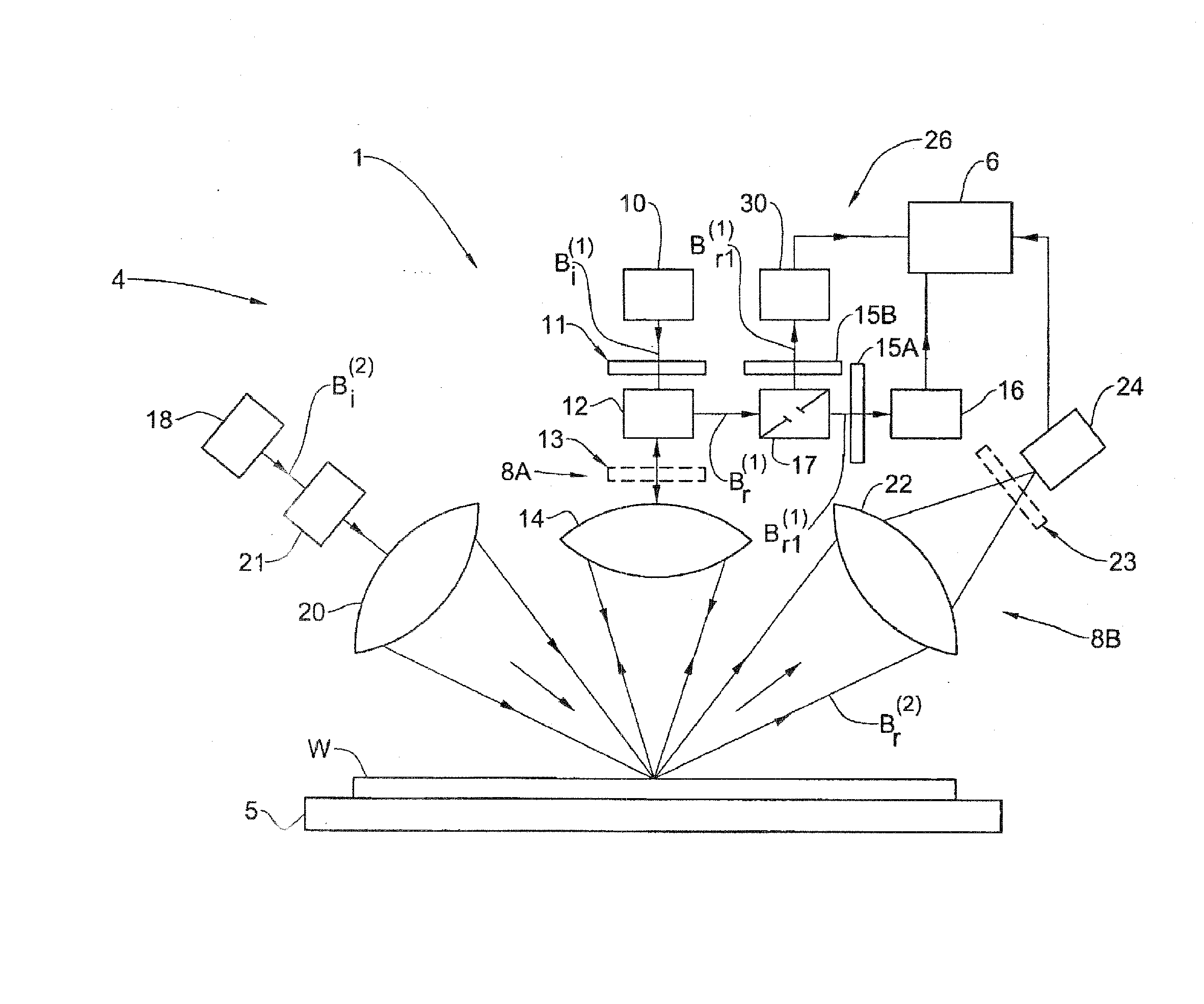
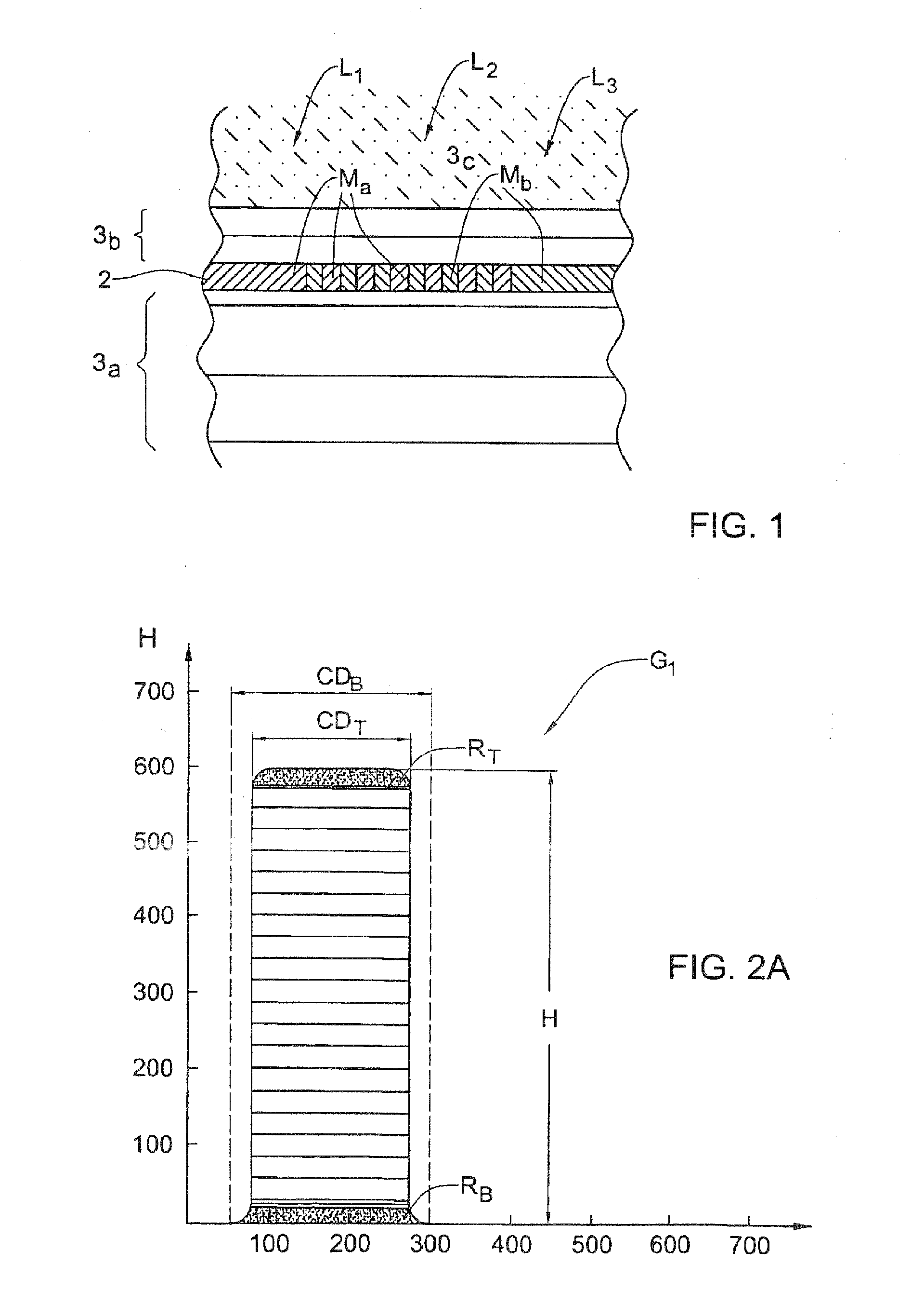
[0053] Referring to FIG. 1, there is illustrated (not in a correct scale) a wafer W that typically has a plurality of stacks formed by different layers, and presents a structure with a periodic pattern. Measurements are aimed at determining the profile of the periodic pattern (“grating”) formed in one or more of the wafer's layers—layer 2 in the present example. Generally, the periodic pattern may involve more than a single layer (which are not specifically shown here), provided that the periodicity in all patterned layers is equivalent. This periodicity may be either one-dimensional (i.e. repeated lines) or two-dimensional periodicity (i.e. finite-area units repeatedly placed on the nodes of a two-dimensional grid). The patterned layer is enclosed between a plurality of un-patterned, underlying layers 3a and a plurality of un-patterned, over-lying layers 3b terminated by a background medium 3c (e.g. air).

[0054] The patterned layer 2 may include both patterned and un-patterned site...


PUM

PropertyMeasurementUnit
widthaaaaaaaaaa
diameteraaaaaaaaaa
diameteraaaaaaaaaa

Abstract

A method and system are presented for determining a line profile in a patterned structure, aimed at controlling a process of manufacture of the structure. The patterned structure comprises a plurality of different layers, the pattern in the structure being formed by patterned regions and un-patterned regions. At least first and second measurements are carried out, each utilizing illumination of the structure with a broad wavelengths band of incident light directed on the structure at a certain angle of incidence, detection of spectral characteristics of light returned from the structure, and generation of measured data representative thereof. The measured data obtained with the first measurement is analyzed, and at least one parameter of the structure is thereby determined. Then, this determined parameter is utilized, while analyzing the measured data obtained with the second measurements enabling the determination of the profile of the structure.

Description

FIELD OF THE INVENTION [0001] This invention is in the field of measurement techniques, and relates to an optical system and method for the accurate measurement of parameters of regular patterned structures. The invention is particularly useful in controlling a lithography process. BACKGROUND OF THE INVENTION [0002] Lithography is widely used in various industrial applications, including the manufacture of integrated circuits, flat panel displays, micro-electro-mechanical systems, micro-optical systems etc. Generally speaking, the lithography process is used for producing a patterned structure. During the manufacture of integrated circuits, a semiconductor wafer undergoes a sequence of lithography-etching steps to produce a plurality of spaced-apart stacks, each formed by a plurality of different layers having different optical properties. Each lithography procedure applied to the wafer results in the pattern on the uppermost layer formed by a plurality of spaced-apart photoresist r...

Claims


Application Information

Patent Timeline
Patent Type & Authority Applications(United States)
IPC IPC(8): G01B11/14G01N21/47G01N21/55G03F1/00G03F7/20
CPCG01B11/24G01N21/4788G03F7/70616G03F1/0092G01N21/55G03F1/84
Inventor FINAROV, MOSHEBRILL
Owner NOVA MEASURING INSTR LTD
Why Eureka
Try Eureka