Polishing compound for copper wirings and method for polishing surface of semiconductor integrated circuit

a technology of integrated circuits and polishing compounds, which is applied in the direction of polishing compositions with abrasives, basic electric elements, electric instruments, etc., can solve the problems of not being fully satisfactory, unable to form a wiring as designed, and the cmp is known to have problems to be solved, etc., to achieve excellent surface state, and good surface polishing

Inactive Publication Date: 2008-03-13
ASAHI GLASS CO LTD +1
View PDF6 Cites 17 Cited by
  • Summary
  • Abstract
  • Description
  • Claims
  • Application Information

AI Technical Summary

Benefits of technology

[0022] According to the present invention, it is possible to realize high precision surface planarization when copper is used as a wiring metal. Therefore, it is possible to obtain a semiconductor integrated circuit having an excellently flat surface state with little dishing and erosion, such being very effective for multi-layering or miniaturization of semiconductor integrated circuits.

Problems solved by technology

If unevenness is present on the surface of the lower layer circuit, the corresponding unevenness will appear also on the surface on which a new circuit is to be formed and will be out of the depth of focus in lithography, whereby it will be difficult to form a wiring as designed.
However, CMP is known to have problems to be solved, such as a phenomenon so-called dishing wherein the wiring portion is removed to be lower than the planarized surface, a phenomenon so-called erosion wherein, along with high densification of metal wirings, a plurality of closely disposed wirings are scraped off together with a neighboring material such as an insulating material, etc.
With respect to dishing and erosion, many means for solution have been proposed (e.g. Patent Document 1), but they have not been fully satisfactory.

Method used


Image

  • Polishing compound for copper wirings and method for polishing surface of semiconductor integrated circuit
  • Polishing compound for copper wirings and method for polishing surface of semiconductor integrated circuit
  • Polishing compound for copper wirings and method for polishing surface of semiconductor integrated circuit

Examples


example 1

[0087] The composition of a polishing compound was as follows.

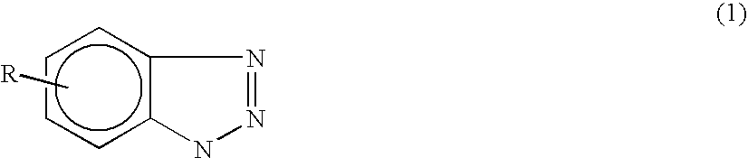
Alumina0.1mass %Tartaric acid (stability constant: 6)1mass %Malonic acid (stability constant: 5)1mass %BTA0.03mass %EDTA (stability constant: 19)0.1mass %Tris(hydroxymethyl)aminomethane3.9mass %Waterthe rest

[0088] To 100 parts by mass of the above composition, 5 parts by mass of a 30% hydrogen peroxide aqueous solution was added to finally adjust the proportion of hydrogen peroxide in the polishing compound to be 1.4 mass %. In Examples 1 and 2, the alumina was 5-alumina, and its average particle diameter was 0.013 μm and its specific surface area was 100 m2 / g.

[0089] With the above polishing compound, polishing was carried out under the following conditions.

Object to be Polished

Blanket Wafer

[0090] A 8-inch wafer (000CUR015, manufactured by Sematech) having a 1,500 nm thick Cu layer formed on a Si substrate by wet plating, was used as a wafer for evaluating a copper removal rate.

Patterned Wafer

[0091] A 8-inch wa...

example 2

[0101] The composition of the polishing compound was as follows.

Alumina0.1mass %Tartaric acid (stability constant: 6)2mass %BTA0.01mass %Tris(hydroxymethyl)aminomethane4.2mass %Waterthe rest

[0102] To 100 parts by mass of the above composition, 3.3 parts by mass of a 30% hydrogen peroxide aqueous solution was added to finally adjust the proportion of hydrogen peroxide in the polishing compound to be 1 mass %.

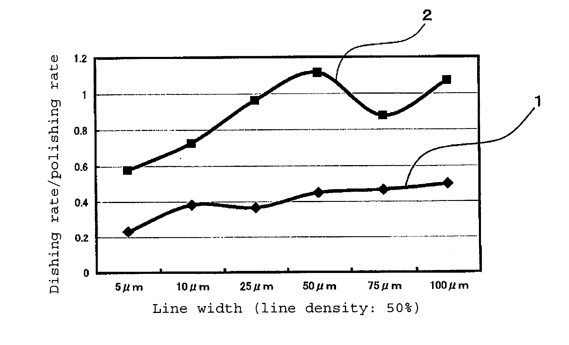
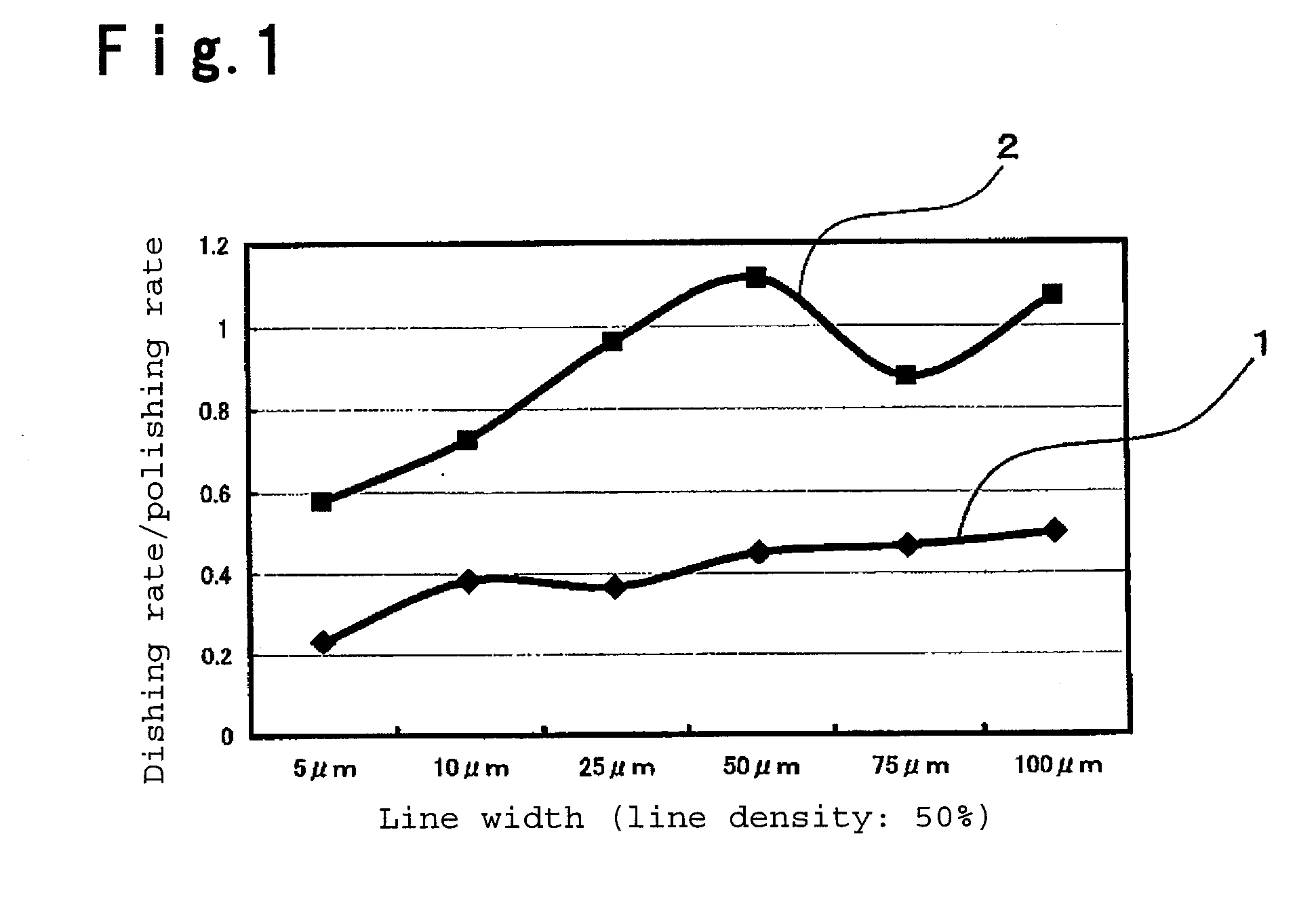
[0103] With the above polishing compound, polishing was carried out under the same conditions as in Example 1 to obtain the results shown in FIG. 1.

[0104] As is evident from the comparison in FIG. 1, in Example 2 wherein no EDTA was incorporated, the ratio of dishing to usual removal rate (dishing rate / polishing rate) is substantially 1 i.e. the polishing speeds being the same at the line widths of at least 25 μm. This means that even if the terminal point of polishing is reached, if the polishing is continued, the removal will proceed with the same removal rate.

[0105] Where...


PUM


Abstract

To provide a technique for realizing high-precision surface planarization when copper is used as a wiring metal. A polishing compound is used which comprises water; a peroxide oxidizer; a surface protective agent for copper; at least one first chelating agent selected from the group consisting of tartaric acid, malonic acid, malic acid, citric acid, maleic acid, oxalic acid and fumaric acid; and at least one second chelating agent selected from the group consisting of triethylenetetramine, ethylenediaminediacetic acid, ethylenediaminetetraacetic acid, tetraethylenepentamine, glycol-ether-diaminetetraacetic acid, trans-1,2-cyclohexanediaminetetraacetic acid, o-phenanthroline, and derivatives thereof.

Description

TECHNICAL FIELD [0001] The present invention relates to a polishing compound for copper wirings and a technique to polish a surface of a semiconductor integrated circuit by using such a polishing compound. BACKGROUND ART [0002] In recent years, in response to increasing needs for high integration of semiconductor integrated circuits, various micro-fabrication techniques have been developed such as miniaturization of semiconductor elements, multi-layering of wirings, etc. [0003] Multi-layering of wirings is meant for forming by means of e.g. lithography a new circuit on a surface having a circuit already formed. If unevenness is present on the surface of the lower layer circuit, the corresponding unevenness will appear also on the surface on which a new circuit is to be formed and will be out of the depth of focus in lithography, whereby it will be difficult to form a wiring as designed. Accordingly, in designing of semiconductor integrated circuits in recent years, it is required to...

Claims


Application Information

Patent Timeline
Patent Type & Authority Applications(United States)
IPC IPC(8): H01L21/302H01L21/461
CPCH01L21/3212C09G1/02
Inventor TSUGITA, KATSUYUKIKAMIYA, HIROYUKI
Owner ASAHI GLASS CO LTD
Why Eureka
Try Eureka