Polishing composition, polishing method, and method for forming copper wiring for semiconductor integrated circuit

a technology of integrated circuits and compositions, applied in the direction of polishing compositions with abrasives, electrical equipment, chemistry apparatuses and processes, etc., can solve the problems of insufficient satisfaction and inability to form wiring patterns, and achieve the effects of low cost, low production cost and low production cos

Inactive Publication Date: 2008-10-23
ASAHI GLASS CO LTD
View PDF7 Cites 11 Cited by
  • Summary
  • Abstract
  • Description
  • Claims
  • Application Information

AI Technical Summary

Benefits of technology

[0021]According to the present invention, it is possible to realize surface flattening with high precision in a case of using copper as a metal for wiring. Accordingly, the present invention enables to obtain a semiconductor int

Problems solved by technology

The increase of the number of wiring layers is to form a new circuit pattern on an existing circuit pattern by using e.g. a lithography, but if there are protrusions or recessed portions are present on a surface of the under layer circuit pattern, protrusions and recessed portions are also formed on a surface of the newly formed circuit pattern, these portions depart from the depth of focus of lithography, and thus, wiring patterns can not be formed as they are designed.
However, in CMP that is a method for flattening a sur

Method used


Image

  • Polishing composition, polishing method, and method for forming copper wiring for semiconductor integrated circuit
  • Polishing composition, polishing method, and method for forming copper wiring for semiconductor integrated circuit

Examples


examples

[0122]Now, the present invention will be described with reference to Examples, but the present invention is by no means limited to these Examples. Examples 1 to 10 and Examples 12 to 19 are Examples of the present invention, and Example 11 is a Comparative Example.

[0123]The composition of each of polishing compositions of Examples 1 to 19 is shown in Table 1. The content of each component is shown in the unit of mass % based on the total of mixed polishing composition. The content of pH adjusting agent required for obtaining a desired pH value is determined in advance by a separate test using a polishing composition having the same composition. The pH value is measured by using a pH meter (pH 81-11) manufactured by Yokogawa Electric Corporation.

[0124]With respect to the polishing composition of each of Examples 1 to 10, first of all, a predetermined amount of 2-pyridinecarboxylic acid (Examples 1 to 3, Examples 5 to 10) or oxalic acid (Example 4), that are the carboxylic acids (B-1)...

example 76

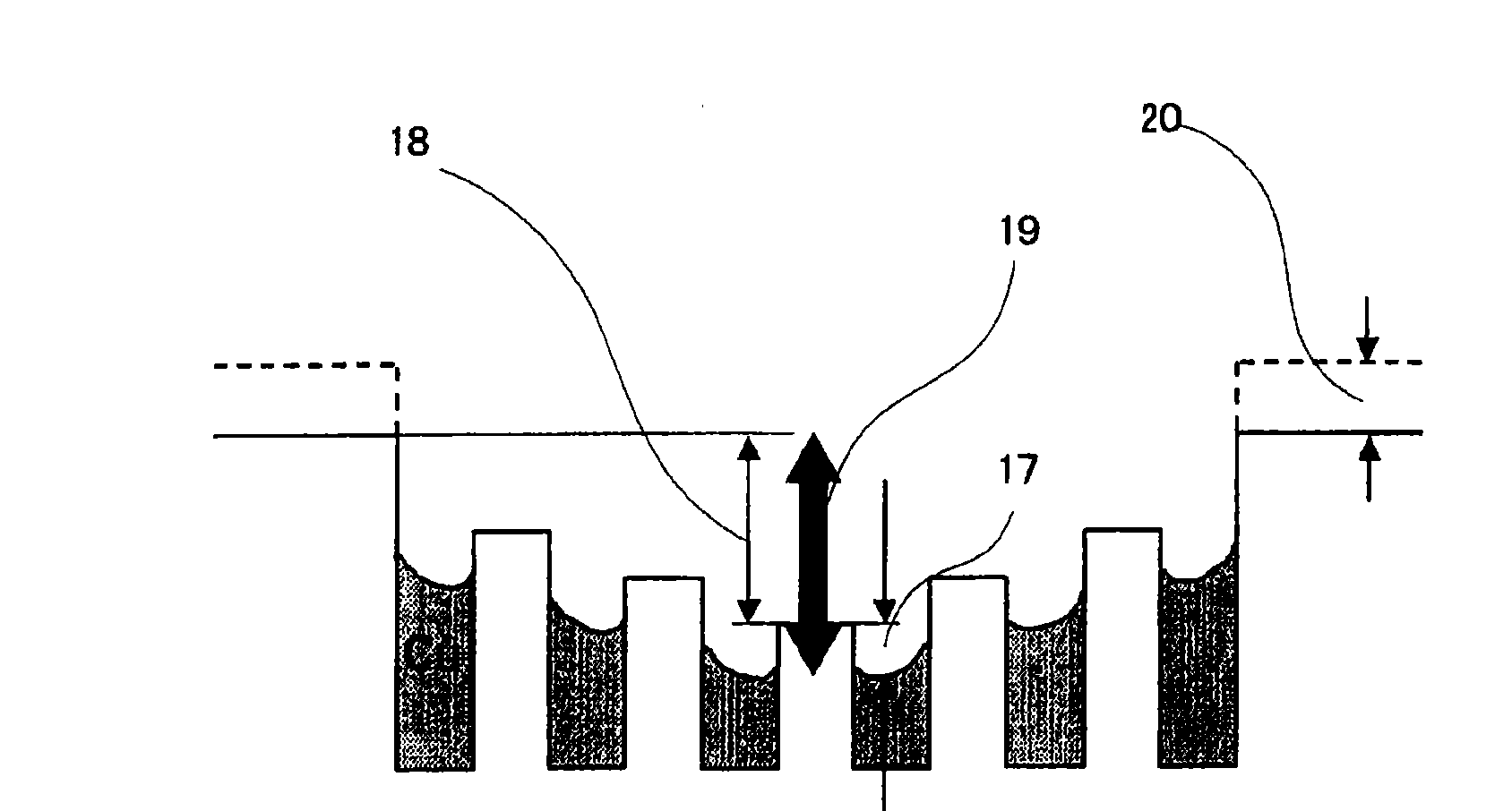
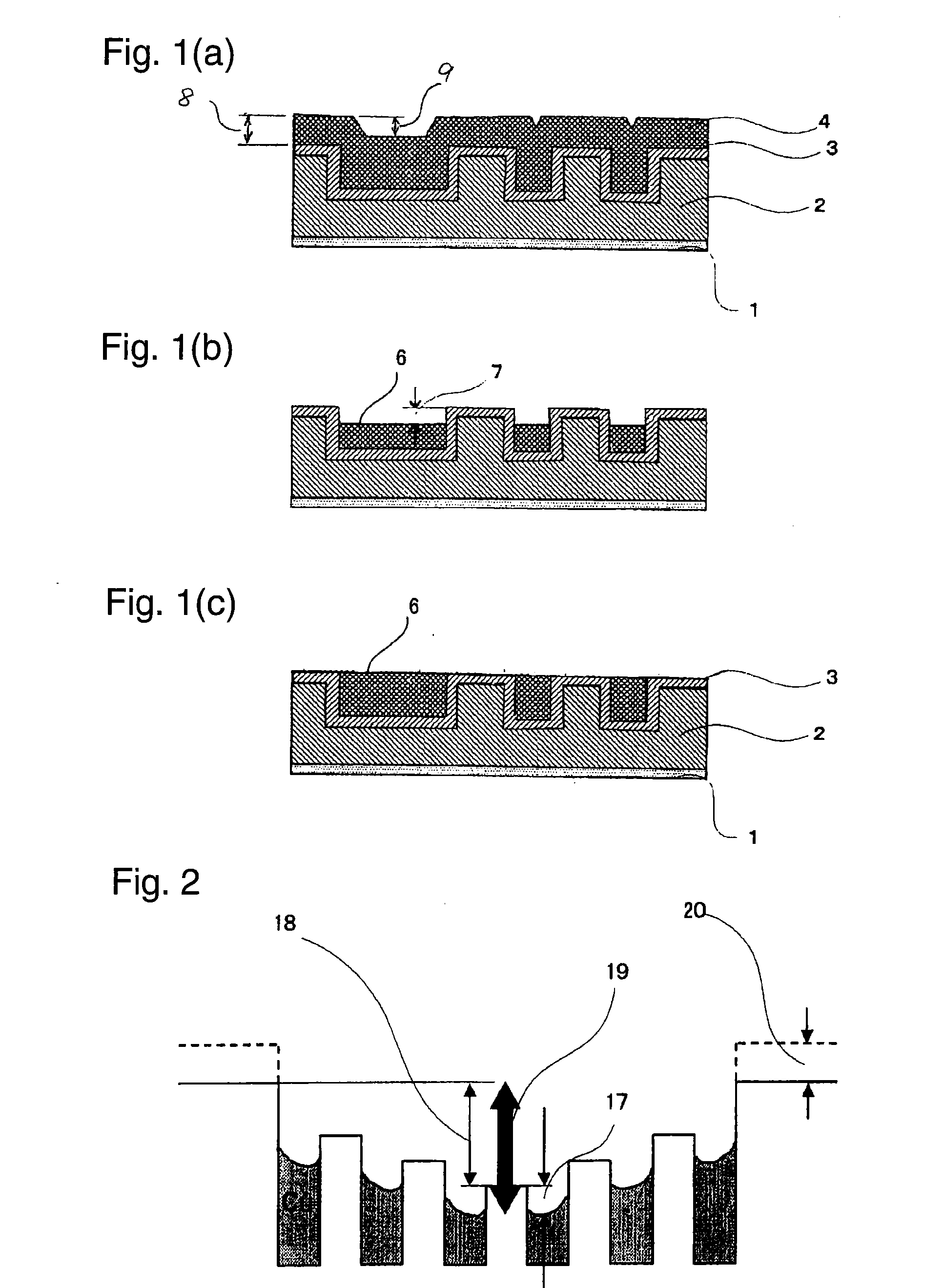
[0169]This example is an example of polishing method in a patterning step of polishing a copper layer formed on an insulation layer via a barrier layer to form alternately arranged copper-buried wirings and insulation layers, wherein the method comprises a first polishing step of polishing the copper layer formed on the insulation layer via the barrier layer by using the polishing composition of the present invention as a first polishing composition, and a second polishing step to be carried out subsequently to the first polishing step.

[0170]A polishing composition for the second polishing step for polishing the barrier layer and the insulation layer was produced in the following manner. Nitric acid, KOH and citric acid were added to a purified water, they were stirred for 10 minutes to obtain an “a” solution. Then, benzotriazole dissolved in ethylene glycol was added to the “a” solution, and pullulan (molecular weight: 2×10⁵) was added to the solution and stirred them for 10 minute...


PUM


Abstract

The present invention provides a technique for realizing highly flat surface of a semiconductor integrated circuit employing copper as a wiring metal.
The present invention provides a polishing composition containing a neutralized carboxylic acid, an oxidizer and water, wherein a part of the carboxylic acid is an alicyclic resin acid (A) and the pH value is within a range of from 7.5 to 12. The alicyclic resin acid is preferably at least one type selected from the group consisting of abietic acid, an isomer of abietic acid, pimaric acid, an isomer of pimaric acid and derivatives of these, or a rosin. Further, the present invention provides a polishing method of semiconductor integrated circuit surface in which a copper film formed on a surface having a groove for wiring, by using the polishing composition, and the present invention provides a copper wiring for semiconductor integrated circuit formed by this polishing method.

Description

TECHNICAL FIELD[0001]The present invention relates to a polishing composition and a technique for polishing a surface of semiconductor integrated circuit by using the polishing composition.BACKGROUND ART[0002]In recent years, to meet needs for high integration of semiconductor integrated circuit, various microfabrication techniques such as reduction of pattern size or increase of the number of wiring layers in a semiconductor element, have been developed.[0003]The increase of the number of wiring layers is to form a new circuit pattern on an existing circuit pattern by using e.g. a lithography, but if there are protrusions or recessed portions are present on a surface of the under layer circuit pattern, protrusions and recessed portions are also formed on a surface of the newly formed circuit pattern, these portions depart from the depth of focus of lithography, and thus, wiring patterns can not be formed as they are designed. To cope with this problem, in the design of semiconducto...

Claims


Application Information

Patent Timeline
IPC IPC(8): C09K13/00H01L21/461
CPCC09G1/02H01L21/3212
Inventor YOSHIDA, IORIKAMIYA, HIROYUKITAKEMIYA, SATOSHIHAYASHI, ATSUSHINAKAZAWA, NORIHITO
Owner ASAHI GLASS CO LTD
Why Eureka
Try Eureka