Method and apparatus for detecting defects

Inactive Publication Date: 2008-03-20
HITACHI HIGH-TECH CORP
View PDF10 Cites 33 Cited by
  • Summary
  • Abstract
  • Description
  • Claims
  • Application Information

AI Technical Summary

Benefits of technology

[0017] The present invention relates to a defect detecting method and apparatus which make it possible to discriminate defects using light that is detected through the almost entire hemispherical surface having a subject of processing as

Problems solved by technology

A conventional apparatus which is based on direct comparison between different dies is described as having the following drawbacks, for example: 1) it is relatively expensive in the case where it requires high mechanical accuracy, 2) the throughput is low, 3) it occupies a large area, 4) it requires a dedicated operator, 5) it is not suitable for in-line inspection (i.e., the apparatus operates for

Method used


Image

  • Method and apparatus for detecting defects
  • Method and apparatus for detecting defects
  • Method and apparatus for detecting defects

Examples


first embodiment

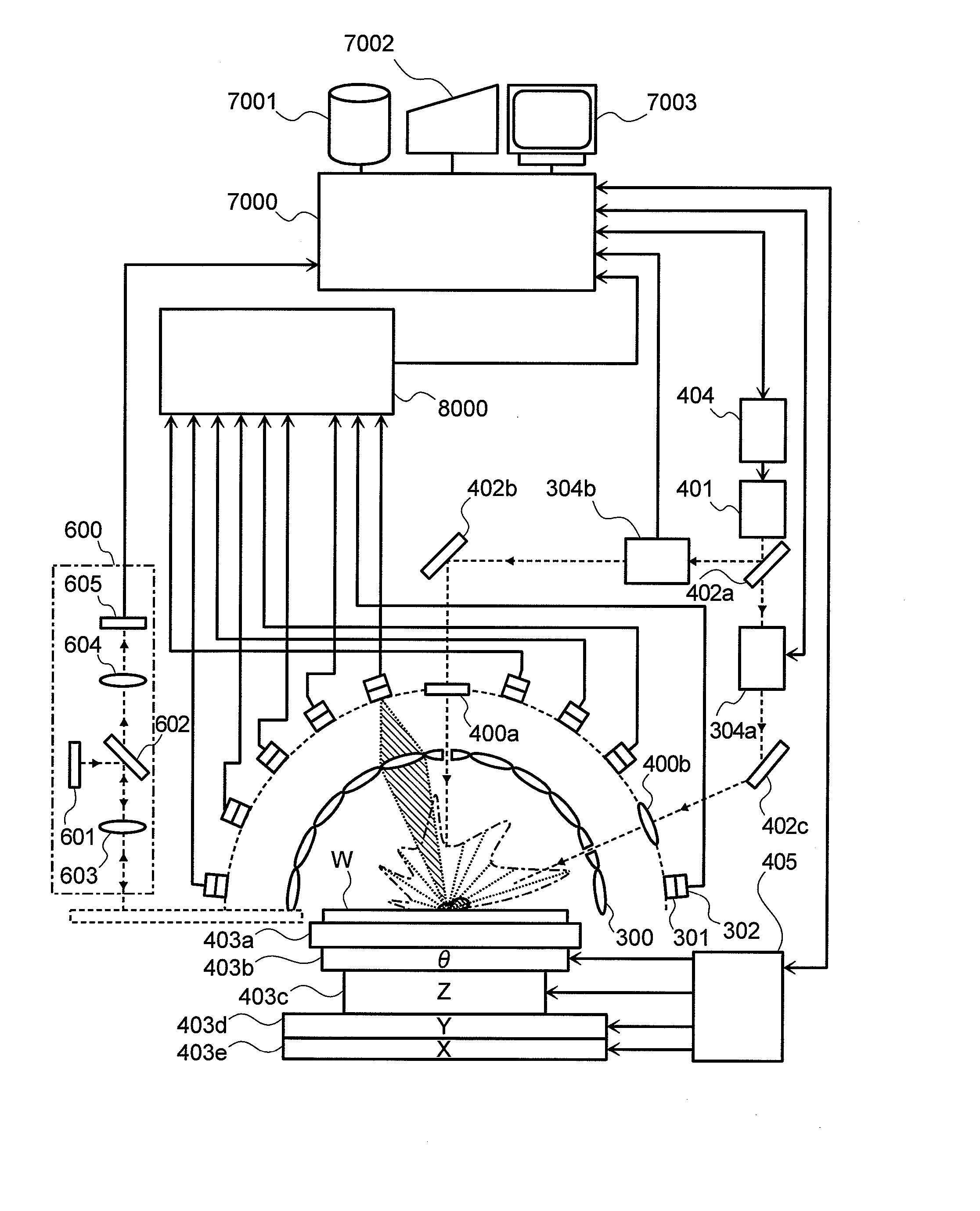
[0079] Next, the invention will be described with reference to FIGS. 1-23. The following description will be directed to detection of defects on a semiconductor wafer.

[0080] First, FIG. 1 shows an exemplary apparatus for detecting defects on a semiconductor wafer. As shown in FIG. 1, the apparatus is composed of a laser light source 401 for emitting laser light, a laser controller 404 for driving the laser light source 401, plural condenser lenses 300 for condensing scattered light coming from an inspection subject (semiconductor wafer) W and defects, 4-segmented polarizing plates 301 each for dividing scattered light detected by the corresponding condenser lens 300 into four polarization components, 4-segmented photodetectors 302 each for detecting the four respective polarization components, a signal processing section 8000, a computer 7000, a storage device 7001, an output device 7002, a display device 7003, a wafer chuck 403a, a θ stage 403b, a Z stage 403c, a Y stage 403d and a...

second embodiment

[0110] In view of the above, in the second embodiment, signals obtained are processed in the following manner. For example, assume that, as shown in FIGS. 30(a) and 31(a), illumination beams are applied to two patterns having different pattern pitches p1 and p2 at the same azimuth angle and elevation angle. In this case, generated diffraction beams have different pitches as shown in FIGS. 30(b) and 31(b). The distributions of diffraction beams at the pupil position are different from each other accordingly as shown in FIGS. 30(c) and 31(c). In the case of FIG. 29(a), the pattern pitch p1 is the same as in the case of FIG. 30(a) but the illumination light is applied at the different azimuth angle than in the case of FIG. 30(a) (φ1=90° in the case of FIG. 29(a) and φ1≠90° in the case of FIG. 30(a)). The distribution of diffraction beams at the pupil position shown in FIG. 29(c) is different from that shown in each of FIGS. 30(c) and 31(c). However, the pitch of the distribution of dif...


PUM


Abstract

A defect detecting apparatus for detecting defects on a substrate sample (wafer) having circuit patterns such as interconnections. The defect detecting apparatus is provided with stages that can be moved arbitrarily in each of the X, Y, Z, and θ directions in a state that the substrate sample is mounted thereon, an illumination optical system for illuminating the circuit patterns from one or plural directions, and a detection optical system for detecting reflection light, diffraction light, or scattered light coming from an inspection region being illuminated through almost the entire hemispherical surface having the substrate sample as the bottom surface. The NA (numerical aperture) thereby falls within a range of 0.7 to 1.0. Harmful defects or foreign substances can be detected so as to be separated from non-defects such as surface roughness of interconnections.

Description

BACKGROUND OF THE INVENTION [0001] The present invention relates to a method and apparatus for detecting foreign substances or defects that occur during manufacture of LSIs or liquid crystal substrates. [0002] Conventional techniques for detecting foreign substances or defects stuck to or generated in a semiconductor wafer or the like are ones using signals that are detected by plural optical systems and plural detectors. These techniques are disclosed in, for example, JP-T-2006-501470 (the symbol “JP-T” as used herein means a published Japanese translation of a PCT application), JP-T-2005-539225, JP-T-2002-519694, JP-A-6-94633, JP-A-6-242012, JP-A-5-332946, and “Multidetector Hemispherical Polarized Optical Scattering Instrument,” 1999 SPIE Proceedings 3784, pp. 304-313. [0003] JP-T-2006-501470 describes a method for inspecting a semiconductor wafer, which is included in the background art of the invention. A system for dark-field-inspecting the surface of a sample such as a semico...

Claims


Application Information

Patent Timeline
IPC IPC(8): G01N21/00
CPCG01N21/21G01N2201/0655G01N21/95623G01N21/95607
Inventor NAKANO, HIROYUKIYOSHITAKE, YASUHIRONAKATA, TOSHIHIKOUENO, TAKETO
Owner HITACHI HIGH-TECH CORP
Why Eureka
Try Eureka