

Electrophotographic photoreceptor, and process cartridge and image-forming apparatus using the same
a technology of photoreceptor and process cartridge, which is applied in the direction of electrographic process apparatus, instruments, coatings, etc., can solve the problems of image blurring, image deformation, image blurring,
- Summary
- Abstract
- Description
- Claims
- Application Information
AI Technical Summary
Benefits of technology
Problems solved by technology
Method used
Image

Examples
example 1
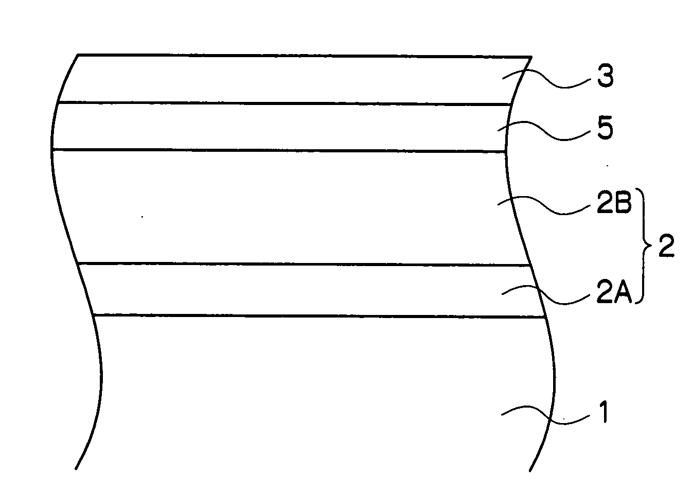
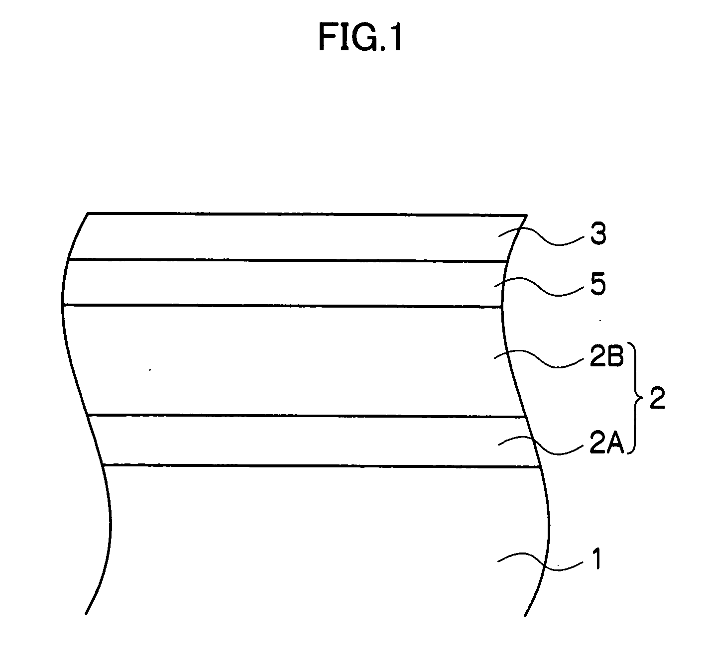
[0307]First, an undercoat layer, a charge-generating layer, and a charge-transporting layer are formed on an Al substrate in this order in the manner described below, to give an organic photoreceptor.
—Formation of Undercoat Layer—
[0308]An undercoat layer having a thickness of 1.0 μm is formed by applying a solution containing 20 parts by weight of a zirconium compound (trade name: Organotics ZC540, manufactured by Matsumoto Chemical Industry Co., Ltd.), 2.5 parts by weight of a silane compound (trade name: A1100, manufactured by Nippon Unicar Co., Ltd.), and 10 parts by weight of a polyvinylbutyral resin (trade name: S-LEC BM-S, manufactured by Sekisui Chemical Co., Ltd.) stirred in 45 parts by weight of butanol on an Al substrate surface having an external diameter of 84 mm and drying the coated film under heat at 150° C. for 10 minutes.
—Formation of Charge-Generating Layer—
[0309]Then, a mixture of 1 part by weight of chlorogallium phthalocyanine as a charge-generating substance, 1...
example 2
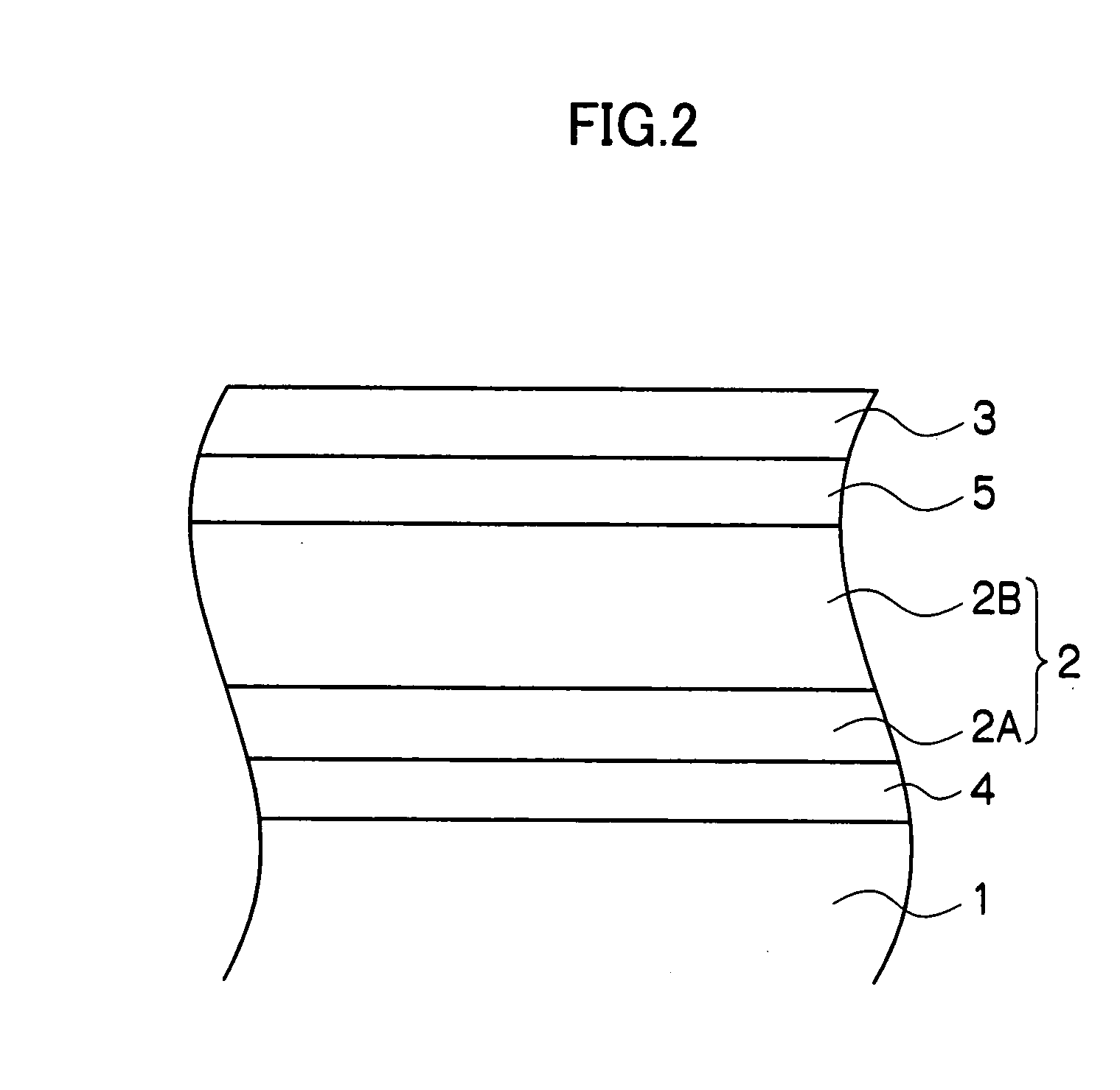
[0326]An organic photoreceptor having an intermediate layer similar to that in Example 1 is prepared; the photoreceptor is placed on a substrate holder 13 in a film-forming chamber 10 of film-forming apparatus, similarly to Example 1; and the film-forming chamber 10 is evacuated through an exhaust vent 11 to a pressure of approximately 0.1 Pa.
[0327]Then, a surface layer is formed on the surface of the intermediate layer-carrying photoreceptor. A mixed gas of nitrogen gas and H2 gas at a ratio of 1:2 is supplied thought a gas-supplying tube 20 into a high-frequency discharge tube unit 21 containing an electrode 19 having a diameter of 50 mm at a flow rate of 300 sccm (nitrogen gas: 100 sccm, hydrogen gas: 200 sccm); a mixed gas of oxygen diluted with helium at a ratio of 100:1 is supplied through the gas-supplying tube 20 at a flow rate of 60 sccm; and a radiofrequency wave of 13.56 MHz is discharged from the flat plate electrode 19 by a high-frequency power supply unit 18 and a matc...
example 3
[0337]First, an organic photoreceptor (non-coated photoreceptor) having an undercoat layer, a charge-generating layer, and a charge-transporting layer formed on an Al substrate in this order is prepared in a similar manner to Example 1.
—Formation of Intermediate Layer—
[0338]An intermediate layer is formed on the non-coated photoreceptor surface in a film-forming apparatus in the configuration shown in FIG. 4.
[0339]First, the non-coated photoreceptor is placed on a substrate holder 13 in a film-forming chamber 10 of film-forming apparatus; the film-forming chamber 10 is evacuated through the exhaust vent 11 at the pressure of up to approximately 0.1 Pa. Then, a mixed gas of nitrogen gas and H2 gas at a ratio of 1:2 is supplied thought a gas-supplying tube 20 into a high-frequency discharge tube unit 21 containing an electrode 19 having a diameter of 50 mm at a flow rate of 300 sccm (nitrogen gas: 100 sccm, hydrogen gas: 200 sccm); and a radiofrequency wave of 13.56 MHz is discharged ...
PUM
| Property | Measurement | Unit |
|---|---|---|
| thickness | aaaaa | aaaaa |
| thickness | aaaaa | aaaaa |
| temperature | aaaaa | aaaaa |
Abstract
Description
Claims
Application Information