Layout design of multilayer printed circuit board

a printed circuit board and multi-layer technology, applied in waveguide devices, pulse techniques, instruments, etc., can solve problems such as error actions, and achieve the effect of reducing the self-impedance and transfer-impedance of multi-layer pcb

Inactive Publication Date: 2008-03-20
INVENTEC CORP
View PDF4 Cites 12 Cited by
  • Summary
  • Abstract
  • Description
  • Claims
  • Application Information

AI Technical Summary

Benefits of technology

[0008]In order to solve the aforementioned problems, the present invention discloses a layout design of a multilayer PCB, which does not only make use of the...

Problems solved by technology

Commonly, the phenomenon resulting from the GBN i...

Method used


Image

  • Layout design of multilayer printed circuit board
  • Layout design of multilayer printed circuit board
  • Layout design of multilayer printed circuit board

Examples


Embodiment Construction

[0019]The detailed features and advantages of the present invention will be described fully in the following part, whose contents will be sufficient to make those skilled in the art appreciate the technological contents of the present invention and implement it thereby, and those skilled in the art can easily appreciate the related objectives and advantages of the present invention according to the contents, claims, and drawings disclosed in the present specification.

[0020]The present invention includes changing the area of the EBG structure of the power layer or the ground layer to reduce the self-impedance and transfer-impedance of the multilayer PCB.

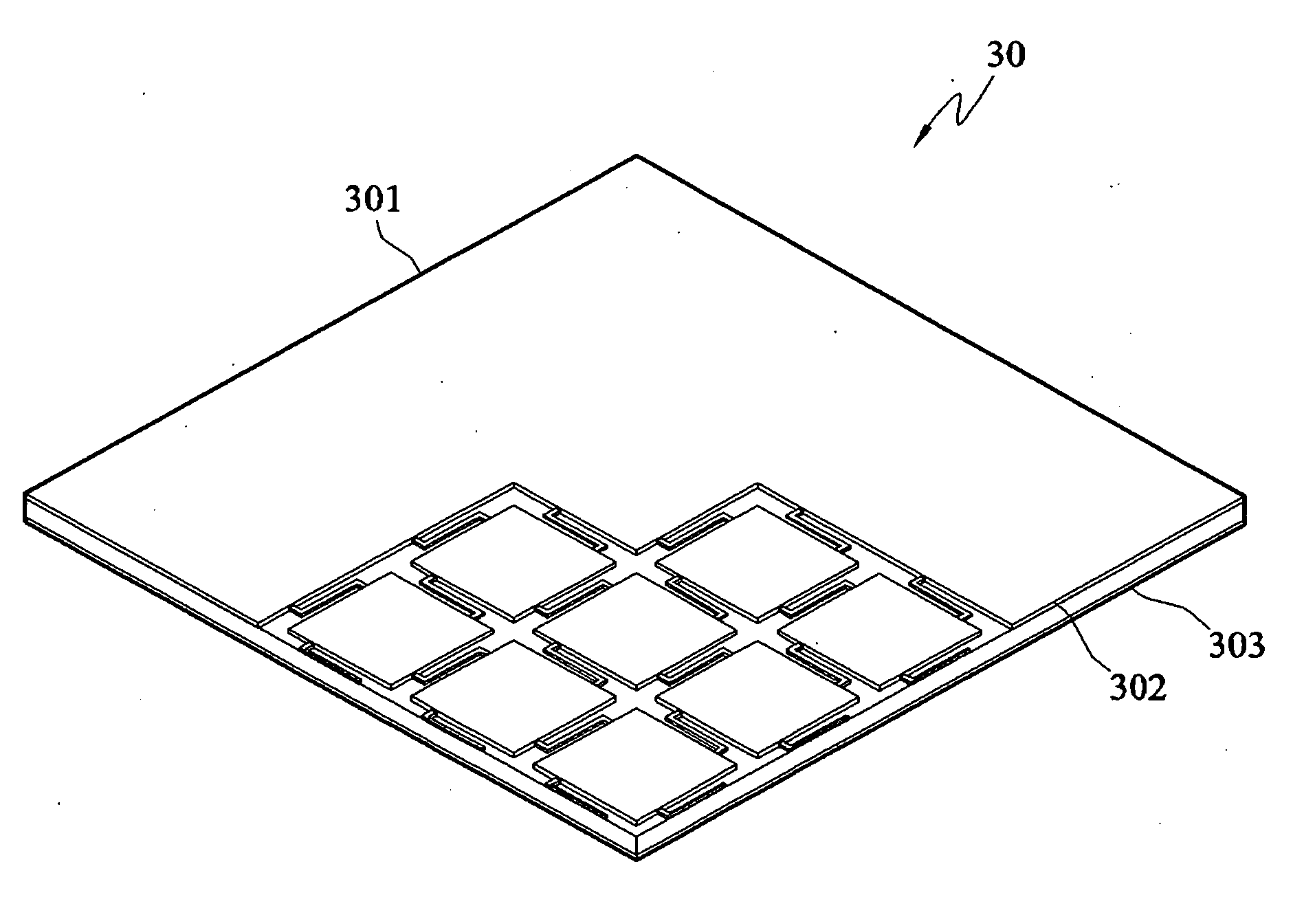
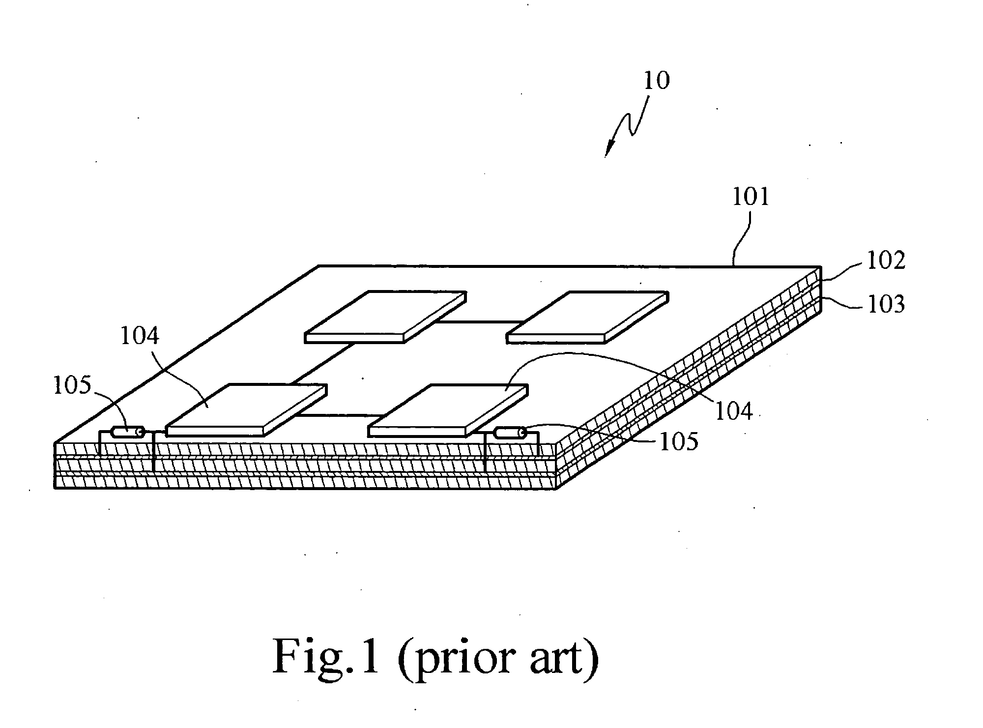
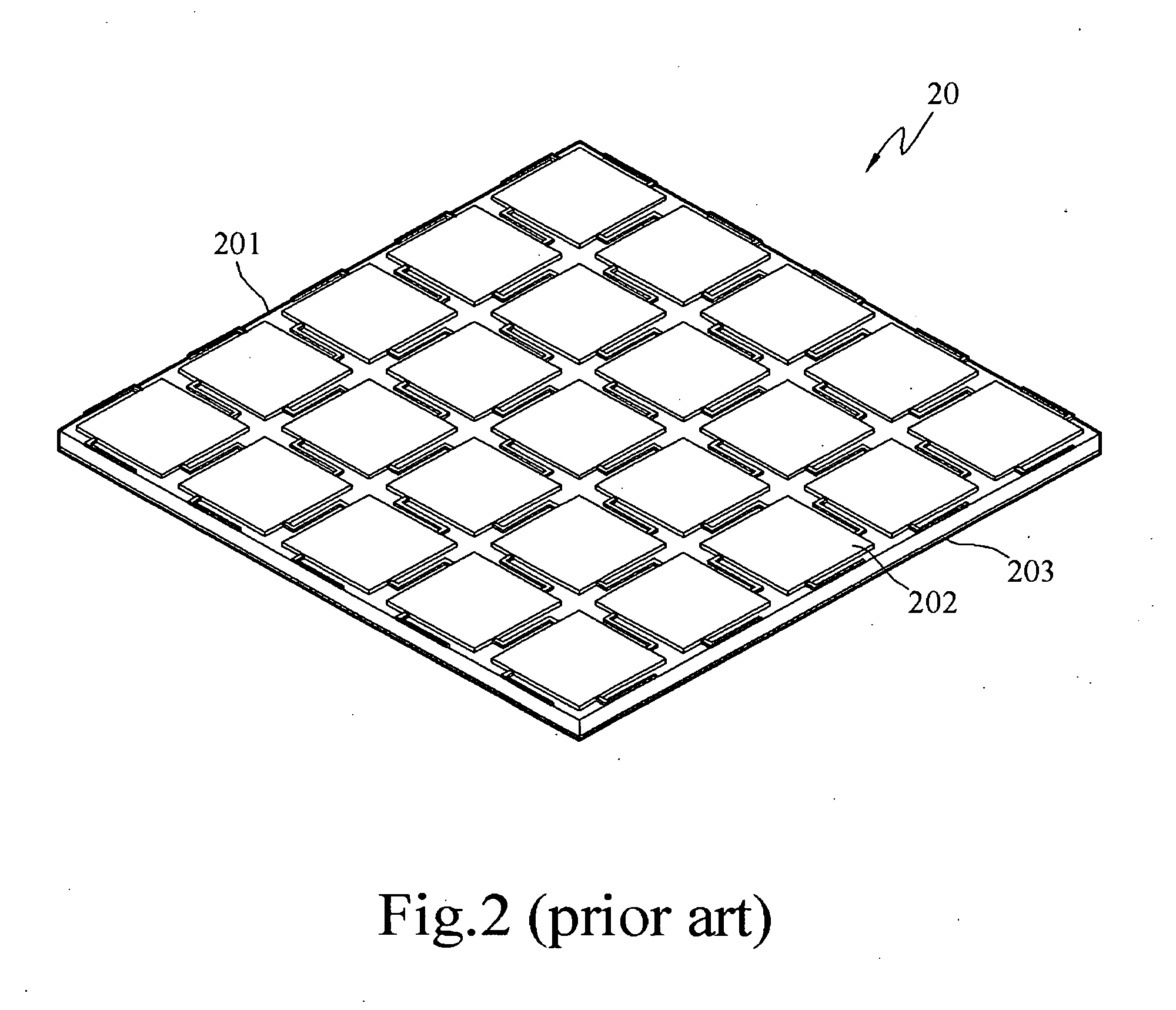
[0021]Please refer to FIG. 3 of a schematic view of the EBG structure according to the present invention. As shown in FIG. 3, the multilayer PCB 301 is formed by laminating a plurality of parallel lamination plates together, in which at least a lamination plate 3011 and a lamination plate 3012 is included. Referring to FIG. 1 again, a...


PUM


Abstract

A layout design of a multilayer printed circuit board (PCB) is provided, which makes use of partial electromagnetic band gap (EBG) structure to constitute a power layer or a ground layer. The EBG structure is mainly used on the linear transmission path from the port of the first integrated circuit to the port of the second integrated circuit on the power layer or the ground layer, so as to overcome the problems concerning self-impedance and transfer-impedance easily occurred in the conventional complete EBG structure.

Description

BACKGROUND OF THE INVENTION[0001]1. Field of Invention[0002]The present invention relates to a multilayer printed circuit board (PCB), and more particular, to a multilayer PCB having an electromagnetic band gap (EBG) structure formed only on the linear transmission path between ports of integrated circuits (IC).[0003]2. Related Art[0004]In the design of high-frequency digital circuits, the trend is toward high speed, small volume, low voltage, and so on. Particularly, under the circumstance that the speed of central processing units (CPU) in personal computer systems has been increasingly improved, the effect of ground bounce noise (GBN) on systems becomes aggravated, so that it is important and necessary to reduce the GBN effect.[0005]The GBN mainly results from high-speed digital circuits, in which the discontinuity of signal line and the parasitic inductance effect of power layer / ground layer cause a transient voltage ΔV in the power layer during the quick switching of an integra...

Claims


Application Information

Patent Timeline
IPC IPC(8): G06F17/50H03K17/693
CPCG06F17/5068H05K1/0231H05K2201/10689H05K2201/09681H05K2201/09972H05K1/0236G06F30/39
Inventor CHEN, YEN-HAO
Owner INVENTEC CORP
Why Eureka
Try Eureka