Electrically Optimized and Structurally Protected Via Structure for High Speed Signals

a high-speed signal and via structure technology, applied in the direction of cross-talk/noise/interference reduction, printed circuit aspects, printed circuit manufacturing, etc., can solve the problems of mechanical weakening, signal not being propagated through the via structure correctly, and mismatching of signals, so as to reduce the capacitance of the via

Inactive Publication Date: 2008-03-27
GLOBALFOUNDRIES INC
View PDF6 Cites 17 Cited by
  • Summary
  • Abstract
  • Description
  • Claims
  • Application Information

AI Technical Summary

Benefits of technology

[0017]The illustrative embodiments provide an electrically optimized and structurally protected via structure for high speed signals in multilayer interconnection substrates, such as printed circuit boards (PCBs), multilayer organic (MLO) packages, multilayer ceramic (MLC) packages, or the like. The v

Problems solved by technology

In modern multilayer interconnection substrate technologies, a problem exists with the via structures in that there typically is an impedance mismatch between the transmission line and the via structure.
Such impedance mismatch causes signals to not be propagated through the via structure correctly.
A problem exists in this alternative via structure, however, in that the structure becomes mechanically weak due to the large areas 202 and 205 of dielectric material where no metal material is provided.
However, w

Method used


Image

  • Electrically Optimized and Structurally Protected Via Structure for High Speed Signals
  • Electrically Optimized and Structurally Protected Via Structure for High Speed Signals
  • Electrically Optimized and Structurally Protected Via Structure for High Speed Signals

Examples


Embodiment Construction

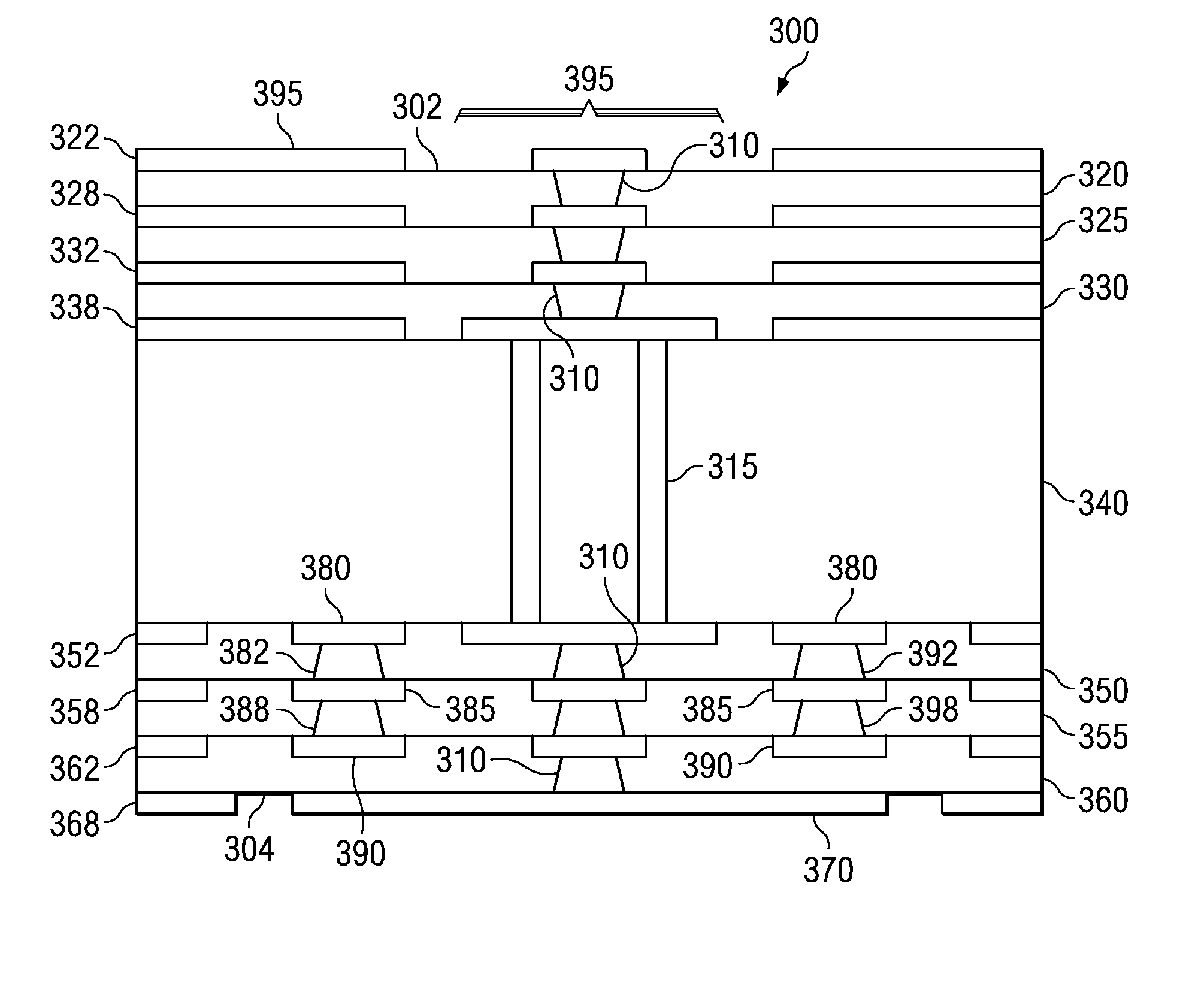
[0036]The illustrative embodiments provide a via structure that is electrically optimized and structurally protected. The via structure and method of manufacturing the via structure as described hereafter may be used in the fabrication of integrated circuit chips, multilayer organic (MLO) packages, multilayer ceramic (MLC) packages, printed circuit boards (PCBs), or any other device that utilizes via structures to electrically connect layers of the device. For purposes of the following description of the illustrative embodiments, it will be assumed that the via structure is utilized with a MLO package. However, the same structures described herein may be used with any multilayer interconnection substrate and are not limited to MLO packages.

[0037]While the following description of the illustrative embodiments will make reference to particular structural elements, it should be appreciated that the structural elements mentioned and their configurations are only exemplary. Many modifica...


PUM


Abstract

An electrically optimized and structurally protected micro via structure for high speed signals in multilayer interconnection substrates is provided. The via structure eliminates the overlap of a contact with the reference planes to thereby reduce the via capacitance and thus, the via impedance mismatch in the via structure. As a result, the via structure is electrically optimized. The via structure further comprises one or more floating support members placed in close proximity to the via within a via clearance area between the via and the reference planes. The floating support members are “floating” in the sense that they are not in electrical contact with either the via or the reference planes. Thus, they are not provided for purposes of signal propagation but only for structural support. The floating support members may be connected to one another by way of one or more microvia structures.

Description

BACKGROUND[0001]1. Technical Field[0002]The present application relates generally to an improved integrated circuit device package. More specifically, the present application is directed to an electrically optimized and structurally protected via structure for high speed signals in multilayer interconnection substrates, such as printed circuit boards, multilayer ceramic packages, and multilayer organic packages.[0003]2. Description of Related Art[0004]Current multilayer interconnection substrates, such as multilayer organic packages or multilayer ceramic packages, and printed circuit board (PCB) constructions require one or more external conductive layers, e.g., circuitry and / or pads for mounting components thereon, and, given today's increased functional demands, a plurality of internal conductive planes, e.g., signal, power and / or ground. To provide effective interconnections between components and the multilayer interconnection substrate's conductive circuitry and pads, the use o...

Claims


Application Information

Patent Timeline
IPC IPC(8): H01L23/48
CPCH01L23/49827H01L23/66H01L2924/0002H01L2223/6616H01L2924/09701H01L2924/3011H05K1/0219H05K1/116H05K3/4602H05K2201/0792H05K2201/09536H05K2201/096H05K2201/09718H05K2201/09781H05K2201/09809H01L2924/00
Inventor HARVEY, PAUL M.KAWASAKI, KAZUSHIGEYAMADA, GEN
Owner GLOBALFOUNDRIES INC
Why Eureka
Try Eureka