Oxidation apparatus and method for semiconductor process

a technology of oxidation apparatus and semiconductor process, which is applied in the direction of solid-state diffusion coating, chemical vapor deposition coating, coating, etc., can solve the problems of poor planar uniformity of film thickness, high oxidation rate, and insufficient use of conventional oxidation methods, so as to simplify and speed up the adjustment operation

Inactive Publication Date: 2008-03-27
TOKYO ELECTRON LTD
View PDF9 Cites 201 Cited by
  • Summary
  • Abstract
  • Description
  • Claims
  • Application Information

AI Technical Summary

Benefits of technology

[0010]An object of the present invention is to provide an oxidation apparatus and method for a semiconductor process, which can...

Problems solved by technology

In this respect, a film formed by wet oxidation under a normal pressure shows a high oxidation rate, but shows poor planar uniformity of film thi...

Method used


Image

  • Oxidation apparatus and method for semiconductor process
  • Oxidation apparatus and method for semiconductor process
  • Oxidation apparatus and method for semiconductor process

Examples


Embodiment Construction

[0027]In the process of developing the present invention, the inventors studied problems of conventional techniques for semiconductor processes, in relation to a method for forming an oxide film by oxidation. As a result, the inventors have arrived at the findings given below.

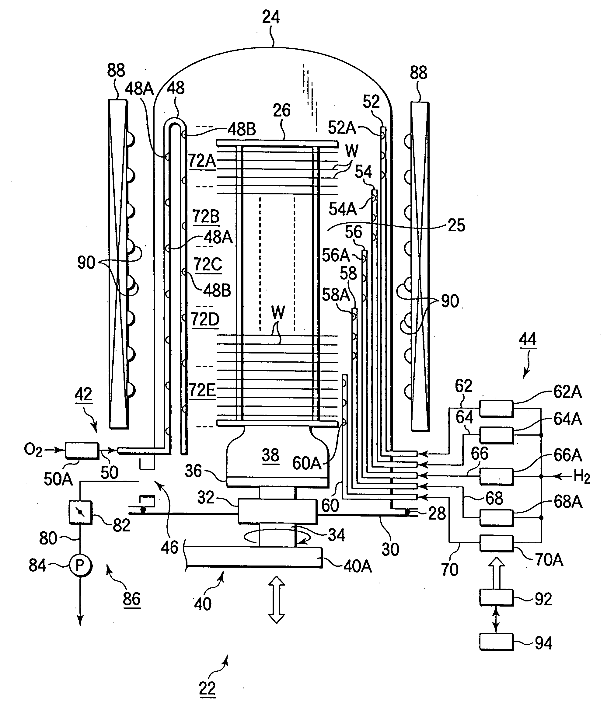
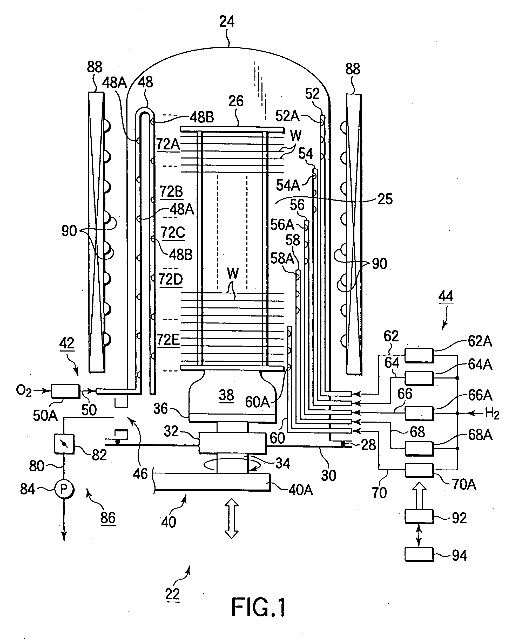
[0028]FIG. 9 is a view schematically showing a conventional vertical heat processing apparatus (oxidation apparatus). The oxidation apparatus includes a process container 2 formed of a quartz cylinder with a ceiling, in which a wafer boat 4 made of quartz is accommodated. The wafer boat 4 can support a plurality of, such as about 25 to 150, semiconductor wafers W at predetermined intervals in the vertical direction. The wafer boat 4 is supported on a heat-insulating cylinder 6, and is moved up and down by a boat elevator (not shown), so that the wafer boat 4 is loaded and unloaded into and from the process container 2 from and to a lower side. The bottom port of the process container 2 is airtightly closed by a...


PUM

PropertyMeasurementUnit
Angleaaaaaaaaaa
Thicknessaaaaaaaaaa
Flow rateaaaaaaaaaa

Abstract

An oxidation apparatus for a semiconductor process includes a process container having a process field configured to accommodate target substrates at intervals vertically, a heater configured to heat the process field; an exhaust system configured to exhaust gas from inside the process field; an oxidizing gas supply circuit configured to supply an oxidizing gas to the process field; and a deoxidizing gas supply circuit configured to supply a deoxidizing gas to the process field. The oxidizing gas supply circuit includes an oxidizing gas nozzle extending over a vertical length corresponding to the process field, and having gas spouting holes arrayed over the vertical length corresponding to the process field. The deoxidizing gas supply circuit includes deoxidizing gas nozzles having different heights respectively corresponding to zones of the process field arrayed vertically, and each having a gas spouting hole formed at height of a corresponding zone.

Description

BACKGROUND OF THE INVENTION[0001]1. Field of the Invention[0002]The present invention relates to an oxidation apparatus and method for a semiconductor process for oxidizing the surface of a target substrate, such as a semiconductor wafer. The term “semiconductor process” used herein includes various kinds of processes which are performed to manufacture a semiconductor device or a structure having wiring layers, electrodes, and the like to be connected to a semiconductor device, on a target substrate, such as a semiconductor wafer or a glass substrate used for an FPD (Flat Panel Display), e.g., an LCD (Liquid Crystal Display), by forming semiconductor layers, insulating layers, and conductive layers in predetermined patterns on the target substrate.[0003]2. Description of the Related Art[0004]In manufacturing semiconductor integrated circuits, a semiconductor substrate, such as a silicon wafer, is subjected to various processes, such as film formation, etching, oxidation, diffusion, ...

Claims


Application Information

Patent Timeline
IPC IPC(8): C23C8/10
CPCC23C8/10H01L21/02238H01L21/67109H01L21/31662H01L21/02255H01L21/02H01L21/00
Inventor INOUE, HISASHITOIYA, MASATAKAMIZUNO, YOSHIKATSU
Owner TOKYO ELECTRON LTD
Why Eureka
Try Eureka