Guided-mode resonance filter and fabrication method of same

a technology of guided-mode resonance and filter, which is applied in the direction of optical light guide, instruments, optics, etc., can solve the problems of power loss, tight fabrication, and inability to keep the traversing light stabl

Active Publication Date: 2008-04-03
NAT CENT UNIV
View PDF1 Cites 3 Cited by
  • Summary
  • Abstract
  • Description
  • Claims
  • Application Information

AI Technical Summary

Problems solved by technology

These filters suffer from various problems such as complex structure with more than 100 individual layers, tight fabrication due to strict tolerance on each layer, and power loss caused by material absorption.
Due to the presence of the grating structure 11, the traversing light is not always kept stable.
However, most of these devices cannot be fabricated on silicon substrates but on lower-index substrates such as quartz, and then, a thin-film structure of higher refractive index is coated as the guided layer.
The utilization of a nonsilicon substrate would restrict the further integration of GMR filters with other optoelectronic devices.

Method used


Image

  • Guided-mode resonance filter and fabrication method of same
  • Guided-mode resonance filter and fabrication method of same
  • Guided-mode resonance filter and fabrication method of same

Examples


Embodiment Construction

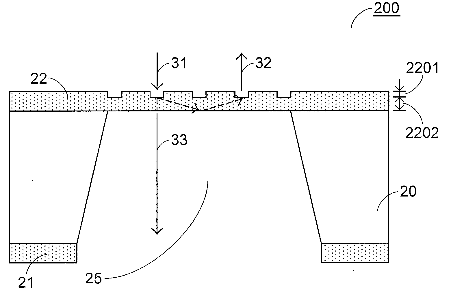
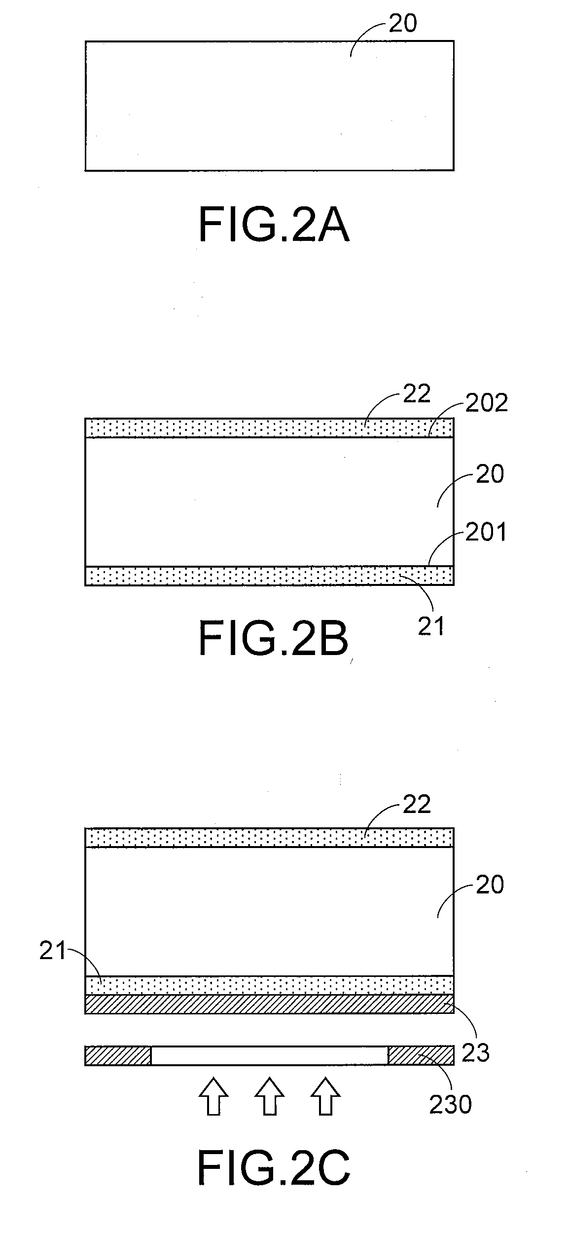
[0027]Referring to FIG. 2A˜2K, a method for fabricating a GMR filter according to an embodiment of the present invention is illustrated. A single-crystal silicon substrate 20 with an arbitrary lattice direction, e.g. (100), and thickness of about 500 μm is first prepared with polishing and RCA chemical cleaning processes, thereby removing impurity and dusts on its surface (FIG. 2A). Highly reflective thin films 21 and 22, e.g. low-stress silicon nitride (SiNx) thin films, are then deposited onto both sides 201 and 202 of the silicon substrate 20 by using a low-pressure chemical vapor deposition (LPCVD) process for an intended thickness, e.g. 1 μm (FIG. 2B). The deposited SiNx film is controlled to be rich in silicon and, hence, a high-refractive-index material. By sequentially spin-coating a photoresist layer 23 and applying a photomask 230 onto the thin film 21 (FIG. 2C), a square hole 231 is patterned. Then, a square hole 211 is opened on the backside SiNx thin film 21 by using ph...


PUM

PropertyMeasurementUnit
thicknessaaaaaaaaaa
thicknessaaaaaaaaaa
latticeaaaaaaaaaa

Abstract

A silicon bulk-micromachining technology is used to fabricate a GMR filter by exploiting the structure of a suspended silicon nitride (SiNx) membrane on the silicon substrate. A first silicon nitride (SiNx) thin film and a second silicon nitride (SiNx) thin film are formed on opposite sides of the silicon substrate. A first opening is defined in the first silicon nitride (SiNx) thin film, and a grating structure is defined in the second silicon nitride (SiNx) thin film. By etching off a portion of the silicon substrate exposed from the first opening until a portion of the second silicon nitride (SiNx) thin film is exposed from the first opening, a light path space is defined.

Description

FIELD OF THE INVENTION[0001]The present invention relates to a guided-mode resonance (GMR) filter, and more particularly to a GMR filter for use in a microelectromechanical system (MEMS) or a microelectroopticalmechanical system (MEOMS). The present invention also relates to a method for fabricating a GMR filter, and more particularly to a method for fabricating a GMR filter by way of a semiconductor manufacturing process.BACKGROUND OF THE INVENTION[0002]Surface and bulk-micromachining techniques have been well developed to fabricate various microelectromechanical system (MEMS) and microelectroopticalmechanical system (MEOMS) structures on the silicon substrate, such as actuators, microheaters, accelerometers, detectors, anemometers, optical transducers such as light switching and optical filtering, and other potential applications. On the other hand, increasing efforts are devoted to the improvement of manufacturing processes for the objectives of proper miniaturization and / or high...

Claims


Application Information

Patent Timeline
Patent Type & Authority Applications(United States)
IPC IPC(8): G02B6/00H01L21/311
CPCG02B6/124G02B6/136G02B6/132
Inventor CHANG, JENQ-YANGWU, MOUNT-LEARNHSU, CHE-LUNGWANG, CHIH-MINGLIU, YUNG-CHIHCHOU, YUE-HONGTSAI, YA-LUNLEE, CHIEN-CHIEH
Owner NAT CENT UNIV
Why Eureka
Try Eureka