Apparatus and method for removing an edge bead of a spin-coated layer

a technology of edge beads and spin-coated layers, which is applied in the direction of coatings, pretreatment surfaces, cleaning using liquids, etc., can solve the problems of difficult control of solvent delivery, yield loss of integrated circuits being built on the wafer, and the proportion of edge beads subsequently detaching from the wafer and becoming a source of particulate contamination

Inactive Publication Date: 2008-04-03
TOKYO ELECTRON LTD
View PDF12 Cites 18 Cited by
  • Summary
  • Abstract
  • Description
  • Claims
  • Application Information

AI Technical Summary

Benefits of technology

[0010]In accordance with an embodiment, an apparatus comprises a substrate support in a coater cup and a nozzle adapted to dispense a material in a liquid phase onto a substrate held by the substrate support. The substrate support is configured to rotate the substrate relative to the coater cup about an azimuthal axis, which spin coats the material in a liquid phase across a top surface of the substrate to form a layer of the material. The apparatus further comprises a head radially moveable relative to the azimuthal axis of the substrate support between a first position in which the head is proximate to a peripheral rim of the substrate and a second position in which the head is retracted from the peripheral rim of the substrate. The head includes a plurality of nozzles adapted to dispense a chemical capable of dissolving the material to contact the layer in an annular region of the layer proximate to the substrate's peripheral rim, when the head is in the first position, and thereby expose the annular region to the chemical.

Problems solved by technology

In practice, however, some excess liquid resist solution tends to collect along the peripheral edge of the wafer as an artifact of the spin-coating process.
Portions of the edge bead may subsequently detach from the wafer and become a source of particulate contamination during subsequent process steps.
Particulate contamination may unfortunately contribute to the yield loss of the integrated circuits being built on the wafer.
However, the delivery of the solvent stream is difficult to control because of factors such as variations in wafer size, the accuracy of centering the wafer in the spin chuck, and positioning errors in locating the nozzle used to spray the solvent stream.
As a result, the radial width of the annular region of the resist removed by the chemical may be difficult to precisely control and is inherently unpredictable.
Conventional chemical edge bead removal processes suffer from several additional shortcomings.
Moreover, the amount of chemical used in conventional edge bead removal processes add to the volume of waste generated in the integrated circuit fabrication process.
The annular width of the removed annular region of resist also reduces the usable area on the top surface of the wafer available for device fabrication.
The relatively large annular width increases in its detrimental effect as devices are scaled to smaller critical dimensions and more densely packed.

Method used


Image

  • Apparatus and method for removing an edge bead of a spin-coated layer
  • Apparatus and method for removing an edge bead of a spin-coated layer
  • Apparatus and method for removing an edge bead of a spin-coated layer

Examples


Embodiment Construction

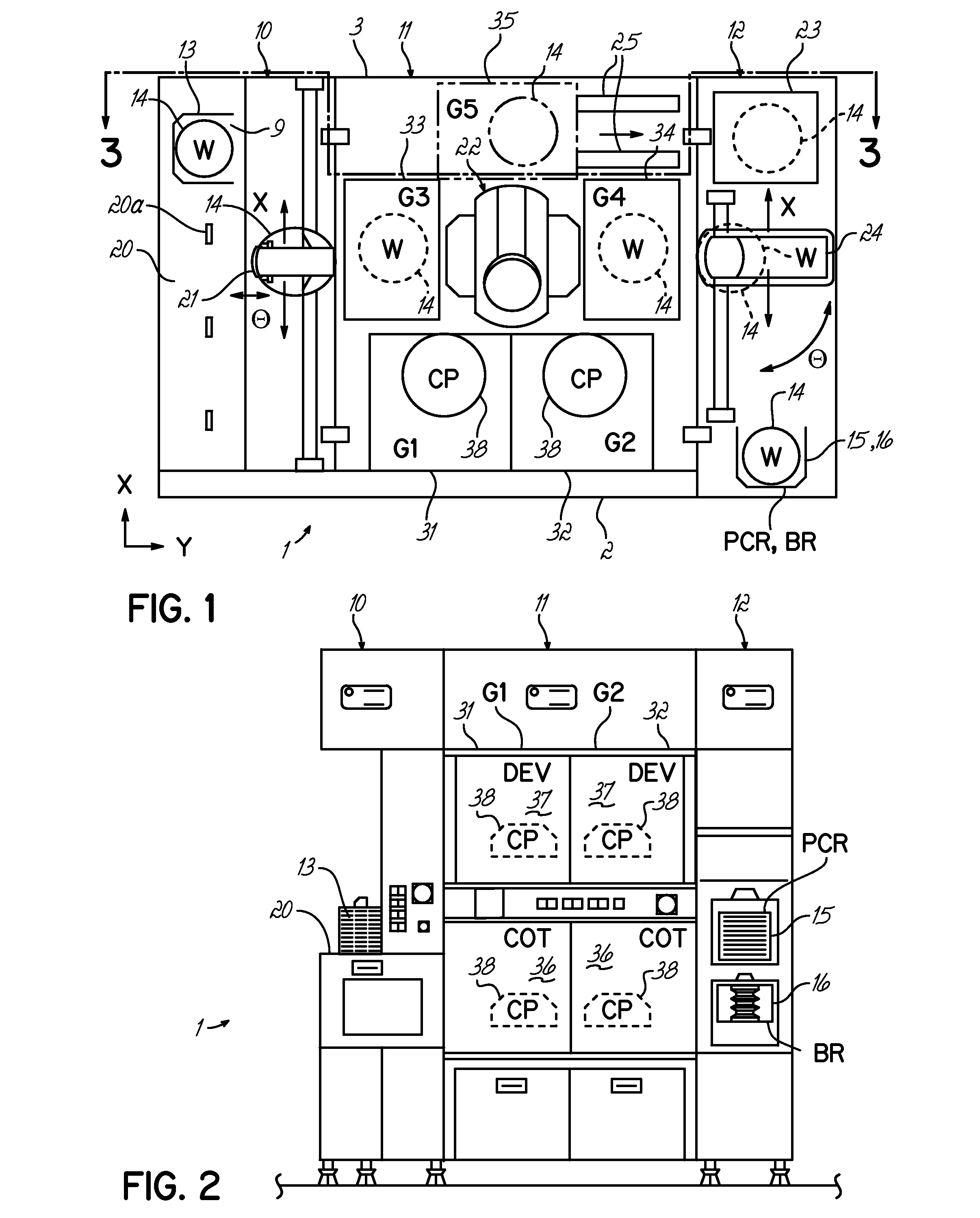
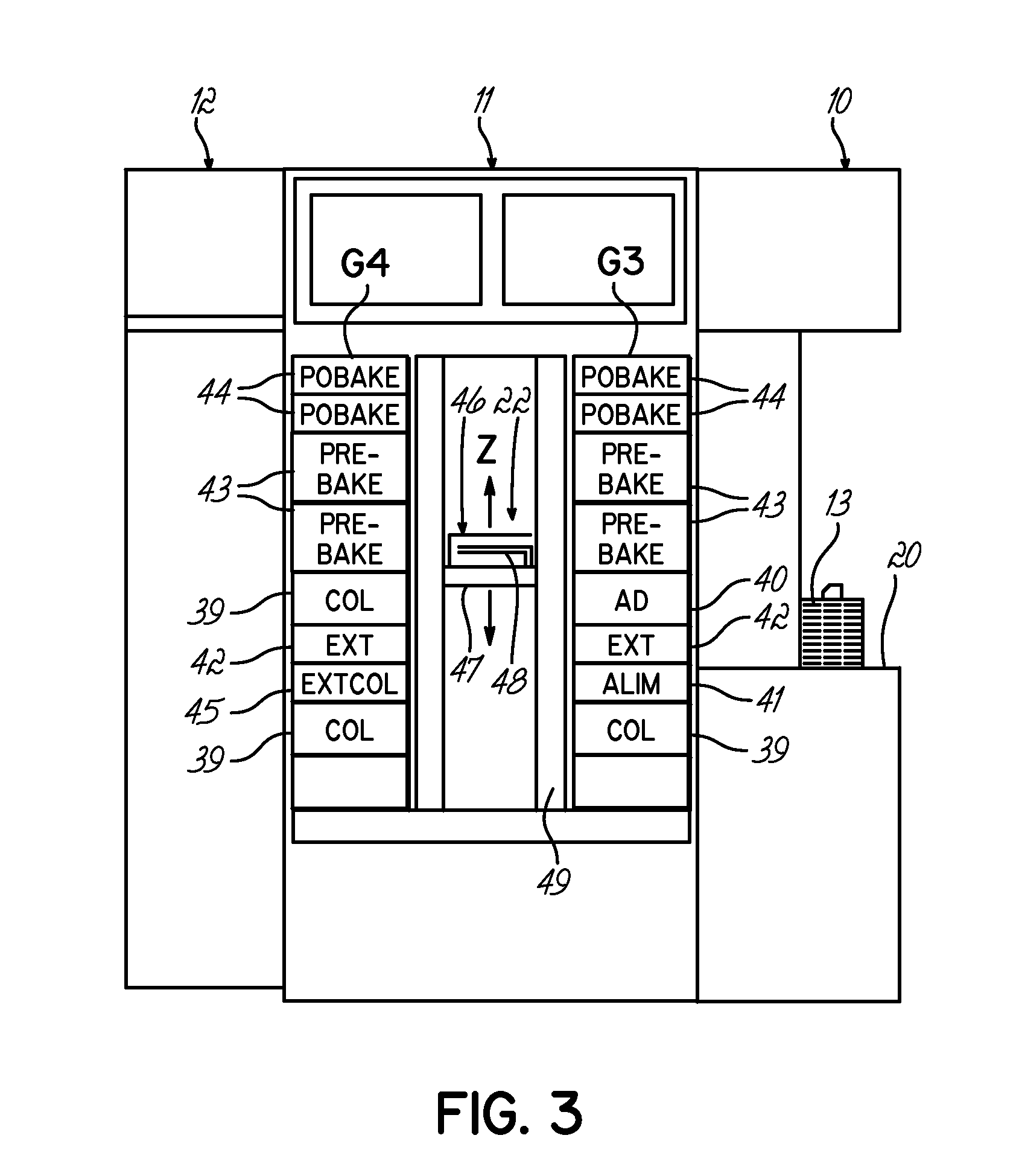
[0019]With reference to FIGS. 1-3, a coating / developing process system 1 comprises a cassette station 10, a process station 11, and an interface section 12, which are contiguously formed as one unit. In the cassette station 10, a cassette (CR) 13 storing a plurality of substrates represented by wafers (W) 14 (e.g., 25 wafers) is loaded into, and unloaded from, the system 1. The process station 11 includes various single-wafer processing units for applying a predetermined treatment required for a coating / developing step to individual wafers (W) 14. These process units are arranged in predetermined positions of multiple stages, for example, within first (G1), second (G2), third (G3), fourth (G4) and fifth (G5) multiple-stage process unit groups 31, 32, 33, 34, 35. The interface section 12 delivers the wafers (W) 14 between the process station 11 and an exposure unit (not shown) that can be abutted against the process station 11.

[0020]A cassette table 20 of cassette station 10 has posi...


PUM


Abstract

An edge bead removal device for a spin coater apparatus and methods of edge bead removal that overcome the deficiencies of conventional edge bead removal techniques. The edge bead removal device includes a coater cup and a head situated within the coater cup proximate to a peripheral edge of a substrate. The head is movable in a radial direction relative to an azimuthal axis of a rotatable substrate support inside the coater cup. The position of the head relative to a rim of the peripheral edge is mapped using an optical sensor. When the substrate support rotates the substrate and the head is used to dispense edge bead removal chemical, the radial position of the head is adjusted, as guided by the map, relative to the azimuthal axis to maintain a constant gap between the head and the substrate's peripheral rim.

Description

FIELD OF THE INVENTION[0001]The present invention relates to apparatus and methods used during the fabrication of semiconductor devices and, in particular, to apparatus and methods for removing an edge bead of a spin-coated layer formed by a spin coating process.BACKGROUND OF THE INVENTION[0002]Semiconductor device fabrication typically involves a number of processes that may be used to form various features and multiple levels or layers of semiconductor devices on a top surface of a semiconductor wafer or another appropriate substrate. For example, lithography is a process that typically involves transferring a prescribed circuit pattern to a resist layer formed on a top surface of the wafer. During the lithography process, the resist layer is formed on the top surface by dispensing a small amount of a liquid resist solution near the center of the wafer, distributing the resist solution across the top surface by a spin-coating process, exposing the resist to radiation in a prescrib...

Claims


Application Information

Patent Timeline
Patent Type & Authority Applications(United States)
IPC IPC(8): B05C13/02B05D3/12
CPCH01L21/6708
Inventor WINTER, THOMAS E.
Owner TOKYO ELECTRON LTD
Why Eureka
Try Eureka