
Nonvolatile Memory Device and Fabrication Method Thereof

a technology of nonvolatile memory and fabrication method, which is applied in the direction of digital storage, semiconductor devices, instruments, etc., can solve the problems of loss of all stored data, difficult to retain data, and even long time-consuming, and achieve the effect of uniform operating characteristics of reram

Active Publication Date: 2008-04-10
SK HYNIX INC
View PDF6 Cites 24 Cited by
  • Summary
  • Abstract
  • Description
  • Claims
  • Application Information

AI Technical Summary

Benefits of technology

[0010]A nonvolatile memory device and its fabrication method may ensure uniform operating characteristics of ReRAM by laminating a resistance layer that determines phase of ReRAM on an upper edge of a lower electrode for obtaining a stable threshold drive voltage level.
[0013]Accordingly, the nonvolatile memory device and its fabrication method may be advantageously used for ensuring uniform operating characteristics of ReRAM by laminating a resistance layer that determines phase of ReRAM on an upper edge of a lower electrode for obtaining a stable threshold drive voltage level.

Problems solved by technology

However, since the DRAM memory cell makes two states “0” and “1” with respect to a charge, it loses all stored data when power is turned off (i.e., a volatile memory device), so it is difficult to retain data.
When a DRAM process is used in the fabrication of the PRAM, an etching operation may be difficult and may even take a long time.
In addition, the memory device uses a transistor or diode for switching, but its structure is complicated and accurate switching operation is not easy.

Method used


Image

  • Nonvolatile Memory Device and Fabrication Method Thereof
  • Nonvolatile Memory Device and Fabrication Method Thereof
  • Nonvolatile Memory Device and Fabrication Method Thereof

Examples


Embodiment Construction

[0020]Hereinafter, preferred embodiments of the present invention will be set forth in detail with reference to the accompanying drawings so that those skilled in the art can easily carry out the invention.

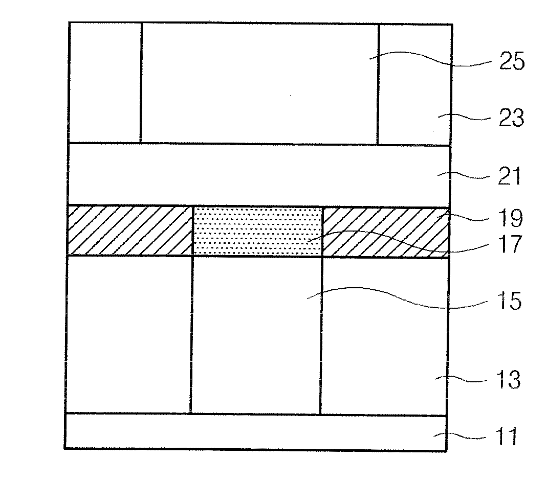
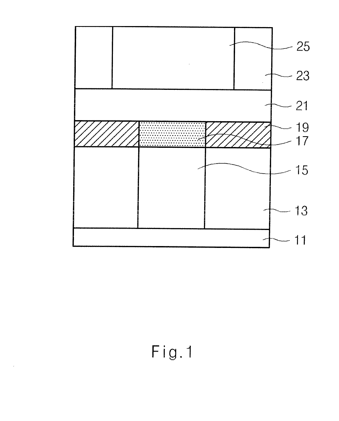
[0021]FIG. 1 is a cross-sectional view showing a method for fabricating a nonvolatile memory device. A first interlayer insulating film 13 is formed on an upper part of a semiconductor substrate 11. The first interlayer insulating film 13 is etched by a photo etching process using a contact mask that defines a lower electrode, to form a lower electrode contact hole (not shown).

[0022]The lower electrode contact hole is filled up with a metal film to form a lower electrode 15. A resistance layer 17 is formed on an upper part of the lower electrode 15. An insulating layer 19 is formed on an upper part of the first interlayer insulating film 13 exclusive of the resistance layer 17. An upper electrode 21 is formed over the resistance layer 17 and over the insulating layer 19. Next, a s...


PUM


Abstract

A nonvolatile memory device and a method for its fabrication may ensure uniform operating characteristics of ReRAM The ReRam may include a laminated resistance layer that determines phase of ReRAM on an upper edge of a lower electrode for obtaining a stable threshold drive voltage level.

Description

CROSS-REFERENCE(S) TO RELATED APPLICATIONS[0001]The present application claims the benefit of priority to Korean patent application number 10-2006-97492, filed on Oct. 4, 2006, the entire contents of which are incorporated herein by reference.BACKGROUND OF THE INVENTION[0002]The present application relates to a nonvolatile memory device and a fabrication method thereof; and, more particularly, to a technology of resistance switching random access memory (ReRAM) using phase changes in resistance.[0003]In general, a semiconductor memory device includes many memory cells being circuitly connected. One exemplary semiconductor memory device is a dynamic random access memory (DRAM). A typical DRAM unit memory cell consists of one switch and one capacitor, and provides benefits such as a high degree of integration and a fast operating speed.[0004]However, since the DRAM memory cell makes two states “0” and “1” with respect to a charge, it loses all stored data when power is turned off (i.e...

Claims


Application Information

Patent Timeline
Patent Type & Authority Applications(United States)
IPC IPC(8): H01L47/00H01L21/00H10N80/00
CPCH01L45/04H01L45/1233H01L45/1666H01L45/124H01L45/1641H01L45/146H10N70/8265H10N70/20H10N70/826H10N70/8833H10N70/041H10N70/061G11C13/0004
Inventor KIM
Owner SK HYNIX INC
Learn More