Oscillation Circuit

a technology of oscillating circuit and oscillating frequency, which is applied in the direction of optical radiation measurement, pulse technique, instruments, etc., can solve the problem of inability to completely stabilize the frequency, and achieve the effect of small frequency variation

Active Publication Date: 2008-04-10
LAPIS SEMICON CO LTD
View PDF5 Cites 21 Cited by
  • Summary
  • Abstract
  • Description
  • Claims
  • Application Information

AI Technical Summary

Benefits of technology

[0010]The object of the present invention is to provide an oscillation circuit havin...

Problems solved by technology

However, since a oscillation frequency of ring oscillator depends on not only the power supply voltage but the ...

Method used


Image

  • Oscillation Circuit
  • Oscillation Circuit
  • Oscillation Circuit

Examples


first preferred embodiment

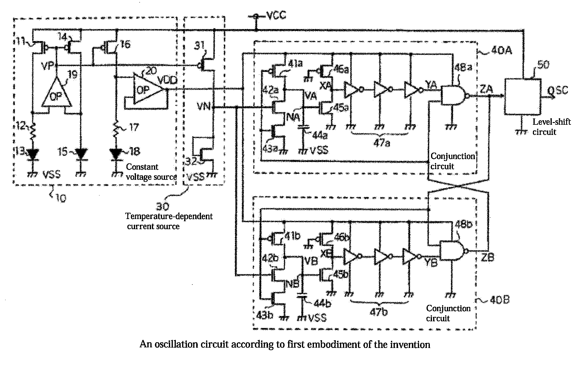
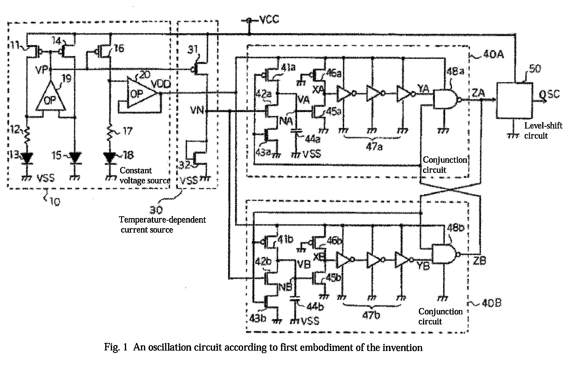
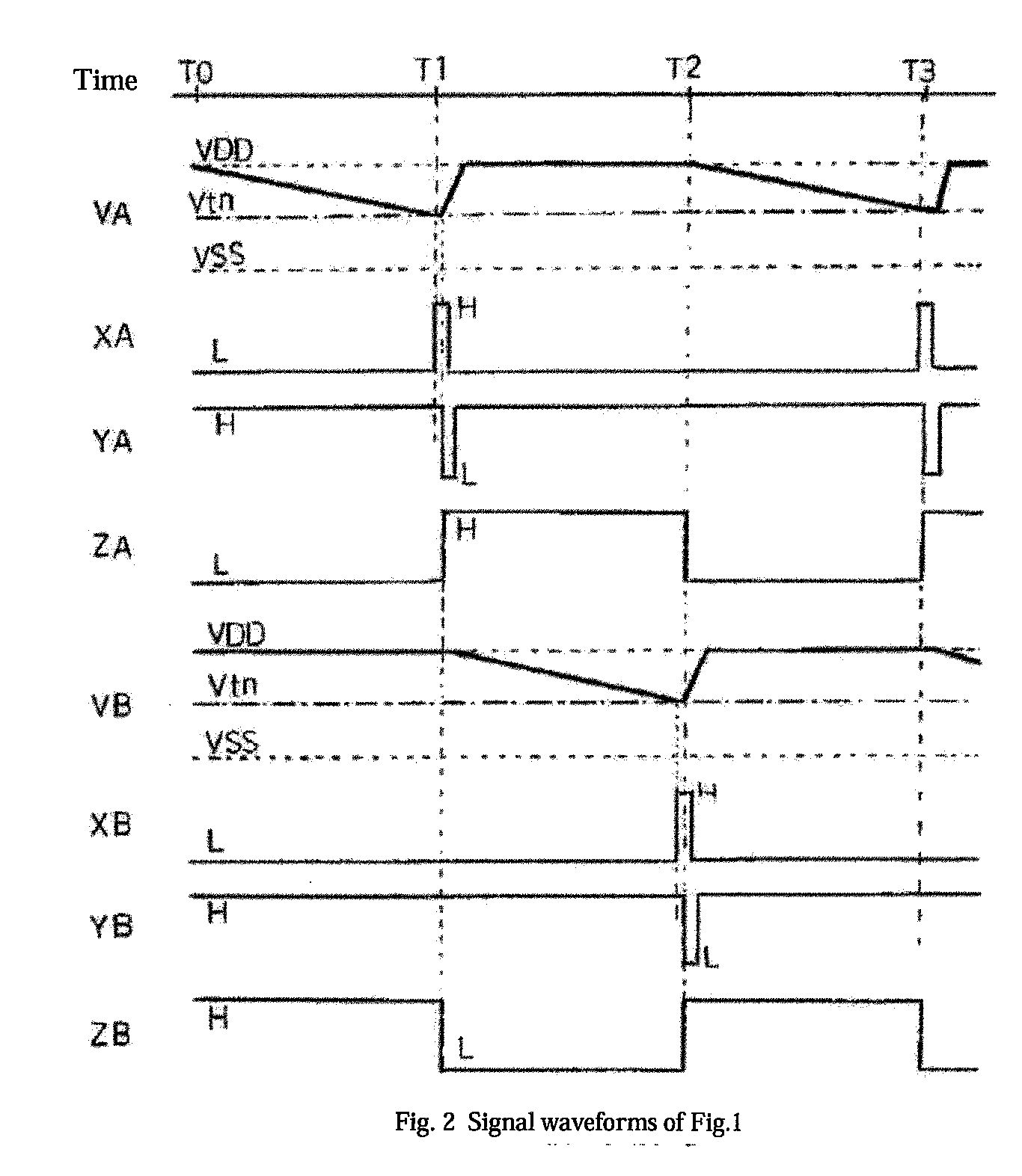
[0018]FIG. 1 is a circuit diagram of the first embodiment of the invention.

[0019]The oscillation circuit is configured by a constant voltage source 10, a temperature-dependent current source 30, a couple of conjunction circuits 40A, 40B composing an astable multi-vibrator.

[0020]The constant voltage source 10 generates a constant voltage VDD independently from the variations of the powers supply voltage VCC and the ambient temperature T.

[0021]The above constant voltage source 10 includes a serial circuit consisting of a P-channel MOS transistor (hereinafter referred to as ‘PMOS’) 11 connected between the power supply voltage VCC node and the ground voltage VSS node, a resistor 12, and a diode 13. Furthermore, a serial circuit of a PMOS 14 and a diode 15 and a serial circuit of a PMOS 16, a resistor 17, and a diode 18 are connected between the power supply voltage VCC node and the ground voltage VSS node. Drains of the PMOSs 11, 14 are connected to a non-inverted input terminal and an...

second preferred embodiment

[0049]FIG. 3 is a circuit diagram of an oscillation circuit according to the second embodiment of the invention. The oscillation circuit consists of a couple of disjunction circuits 70A, 70B composing a temperature-dependent current source 60 and the astable multi-vibrator.

[0050]The temperature-dependent current source 60 generates the voltage VP corresponding to the temperature and includes a serial circuit consisting of a PMOS 61 connected between the power supply voltage VCC node and the ground voltage VSS node, a resistor 62, and a diode 63. Furthermore, a serial circuit consisting of a PMOS 64 and a diode 65 is connected between the power supply voltage VCC node and the ground voltage VSS node. The drains of PMOSs 61, 64 are connected to a non-inverted terminal and a inverted terminal of an operational amplifier 65, respectively. The voltage VP from the output terminals of the above operational amplifier 66 is provided the gates of PMOSs 61, 64 and simultaneously outputted as a...


PUM


Abstract

An output signal ZA of NAND 48a is given to a first input of NAND 48b and is given to a second input of the above NAND 48b, simultaneously through a delay circuit. Furthermore, an output signal ZB of the NAND 48b is given to the first input of NAND 48a and is given to the second input of NAND 48a, simultaneously through a delay circuit. The delay circuit includes a charging and discharging circuit consisting of a NMOS 42 having the conductivity controlled by a voltage VN depending on a temperature signal from a temperature-dependent current source 30 and a capacitor 44, and a NMOS 45 being turned on/off by the voltage of the above capacitor 44. By setting temperature characteristics of the voltage VN and temperature characteristics of the threshold voltage of the NMOS 45 so as to cancel each other, the oscillation frequency variation of the oscillation circuit consisting of astable multi-vibrators can be restrained.

Description

BACKGROUND OF THE INVENTION[0001]1. Field of the Invention[0002]The present invention relates to an oscillation circuit having smaller oscillation frequency variation caused by power supply voltages or ambient temperatures.[0003]This is a counterpart of Japanese patent application Serial Number 273643 / 2006, filed on Oct. 5, 2006, the subject matter of which is incorporated herein by reference.[0004]2. Description of the Related Art[0005]Patent document 1: Japanese Patent Kokai Number 2003-4547[0006]Patent document 2: Japanese Patent Kohyo Number 2005-533443[0007]In the above document 1, there is a description of the temperature detecting circuit for outputting a temperature signal by comparing frequencies between the ring oscillator changing the oscillation frequency corresponding to the ambient temperature and the crystal oscillator.[0008]Furthermore, in the above document 2, there is a description of the constant current circuit for supplying a constant current independently from ...

Claims


Application Information

Patent Timeline
IPC IPC(8): G05D23/20
CPCH03K3/011H03L1/00H03K3/03
Inventor NOGUCHI, MINEO
Owner LAPIS SEMICON CO LTD
Why Eureka
Try Eureka