
Stress measurement method

a stress measurement and stress technology, applied in the field of stress measurement method, can solve the problems of difficult to accurately measure the stress applied to a micro-structure of smaller than a m order or a thin film, take time to conduct measurement, and take time to measure the stress, etc., to achieve shorten the time required for measurement, and improve the accuracy of measurement.

Inactive Publication Date: 2008-04-10
HORIBA LTD
View PDF4 Cites 10 Cited by
  • Summary
  • Abstract
  • Description
  • Claims
  • Application Information

AI Technical Summary

Benefits of technology

[0012]Then the present claimed invention intends to make it possible to measure and to accurately measure stress applying to a micro-structure of several dozen nm˜μm order or a thin film with merits of the Raman spectroscopy that can conduct measurement in a short period of time nondestructively.
[0021]On the other hand, in accordance with this invention, an accuracy of measurement can be spectacularly improved since the stress applied to the measurement area is evaluated based on the stress originated data of a local portion whose area is smaller than that of the measurement area.
[0022]In addition, in case of measuring a big area like this invention, an effect that the time required for measurement is shortened becomes especially clear. For example, in case of measuring a distribution of stress applying to a big area, conventionally each stress has to be measured for each location in the big area by conducting a mapping measurement or the like. On the other hand, in accordance with this invention, since a local stress (or a value associated with the local stress) can be obtained based on the correlation data just by measuring a Raman spectrum once from the entire big area, it becomes possible to omit a mapping measurement, thereby to substantially shorten the time required for measurement.

Problems solved by technology

However, since the XRD has a spatial resolution of several dozen μm at most, it is difficult to measure the stress applying to a micro-structure of smaller than a μm order or a thin film accurately.
Furthermore, there is a problem that it takes time to measure the stress.
However, since a broken measurement specimen has to be prepared separately, there are some problems such that it takes time to conduct measurement and the measurement specimen does not coincide with an actually manufactured device in a precise sense.
Accordingly, if the above-mentioned XRD or CBED is actually applied to measurement of stress in a process line, the time required for measurement becomes a big bottleneck.
With this method, however, a measurable area by using a microscope is about 1 μm at the minimum and an area smaller than 1 μm is difficult to measure.

Method used


Image

  • Stress measurement method
  • Stress measurement method
  • Stress measurement method

Examples


Embodiment Construction

[0035]One embodiment of this invention will be explained with reference to drawings.

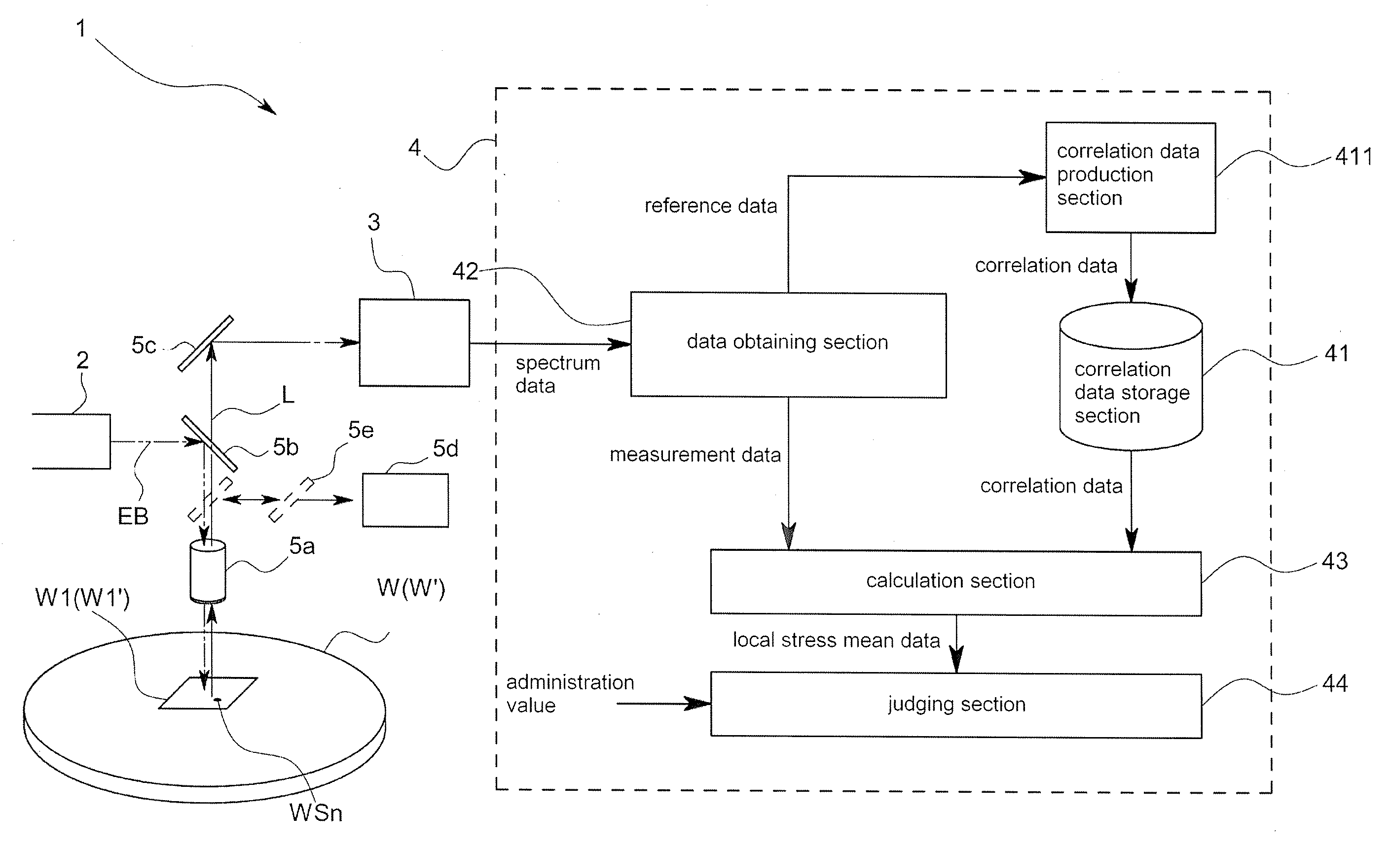
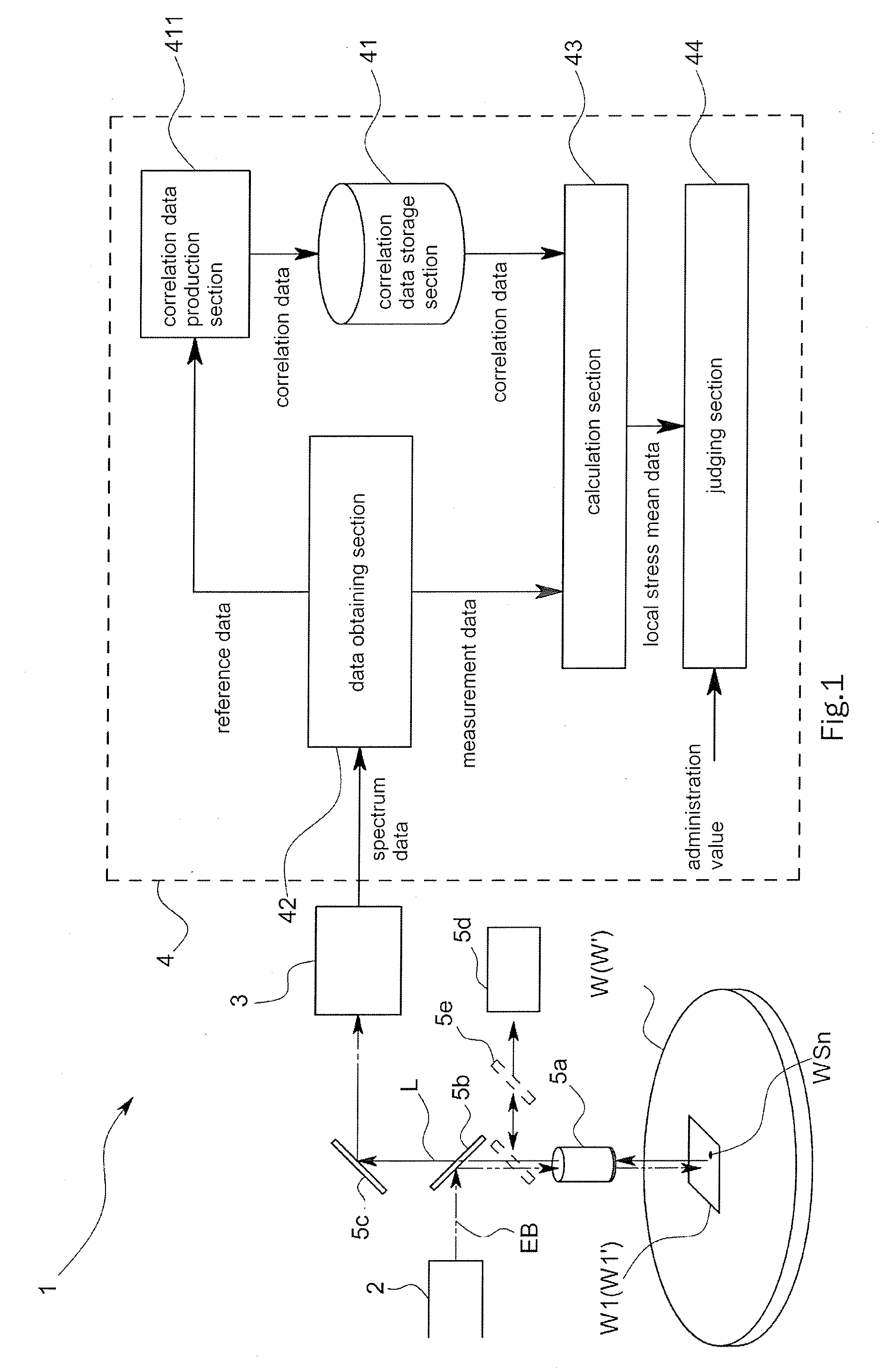
[0036]Stress measurement apparatus 1 in accordance with this embodiment measures stress in a measurement area of, for example, a semiconductor measurement specimen whose shape and composition are standardized in a nondestructive manner. As its pattern structural diagram is shown in FIG. 1, the stress measurement apparatus 1 comprises a laser device 2 as being an energy line irradiation device, a sensor unit 3 that receives Raman scattering light L and an information processing unit 4.

[0037]Each section will be explained in detail. The laser device 2 irradiates laser EB whose excitation wavelength is, for example, 363.8 nm as being energy lines. An irradiation object (detail will be explained later) is a predetermined area W1 of a reference specimen W, multiple (n) portions WS1˜WSn in the predetermined area W1 or a measurement area W1′ of a measurement specimen W′.

[0038]The sensor unit 3 receives the ...


PUM


Abstract

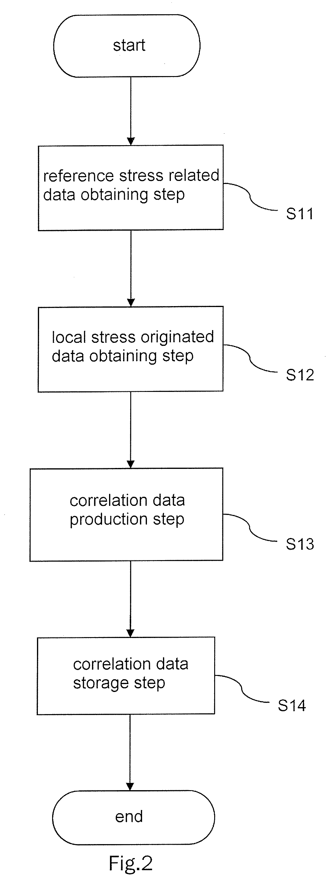
An object of this invention is to provide stress measurement method that is stress of the measuring object nondestructively in a short period of time.In order to attain this object, the stress measurement apparatus 1 comprises a correlation data storage section 41 that analyzes a correlation between reference stress related data obtained from a Raman spectrum L of an entire predetermined area W1 of a reference specimen W and local stress originated data as being data obtained based on a local stress each of which applies to multiple positions WS1˜WSn respectively in the predetermined area W1 and stores correlation data indicating the correlation, a data obtaining section 42 that obtains measurement stress related data from a Raman spectrum L on an entire measurement area W1′, corresponding to the predetermined area W1, of a measurement specimen WS′, and a calculation section 43 that calculates local stress originated data in the measurement area W1′ based on the correlation data and the measurement stress related data.

Description

BACKGROUND OF THE INVENTION AND RELATED ART STATEMENT[0001]The present claimed invention relates to stress measurement method especially preferably used for measuring stress of a measurement specimen whose shape and composition are standardized to a certain degree such as a mass-produced semiconductor substrate and devices.[0002]In order to measure stress applying to a specimen in a process line, it is required to measure the specimen nondestructively in a short period of time. Furthermore, in a field of, for example, semiconductor manufacturing, recently a request has been arising for measuring stress applying to micro-structures smaller than μm order or thin films accurately.[0003]As a method for measuring stress applying to a specimen, there are the XRD (the X-ray Diffraction) and the CBED (the Convergent Beam Electron Diffraction) as shown in the patent document 1 or the patent document 2.[0004]In accordance with the XRD, the stress can be measured without destroying the specime...

Claims


Application Information

Patent Timeline
Patent Type & Authority Applications(United States)
IPC IPC(8): G01B11/16
CPCG01N21/65G01L5/0047G01J3/44G01L1/24G01N21/9501
Inventor NAKA, NOBUYUKIKASHIWAGI, SINSUKE
Owner HORIBA LTD
Learn More