Method and apparatus of scanning a sample using a scanning probe microscope

a scanning probe and sample technology, applied in the direction of mechanical roughness/irregularity measurement, instruments, semiconductor/solid-state device testing/measurement, etc., can solve the problems of poor tracking of the flat-to-sidewall transition, difficult to obtain information regarding the transition region with standard cd mode afm, and difficulty in obtaining reliable data. , to achieve the effect of accurate tracking and high scan velocity

Active Publication Date: 2008-04-17
BRUKER NANO INC
View PDF29 Cites 13 Cited by
  • Summary
  • Abstract
  • Description
  • Claims
  • Application Information

AI Technical Summary

Benefits of technology

[0038]According to another aspect of this preferred embodiment, the method scans five measurement sites of a semiconductor wafer in less than about ten minutes for slow applications to three minutes for faster measurement applications. In pa...

Problems solved by technology

As throughput requirements increase, increased data acquisition speeds are desired, thus making the ability to obtain reliable data a challenge.
However, due to the dynamics of the system, including limitations associated with the scanner, information regarding these transition regions is often difficult to obtain with standard CD mode AFM.
Although the feedback loop or servo command signal to the scanner instructs the scanner to stop, the scanner continues to carry the tip further towards the sidewall 54, as noted above, thus causing poor tracking of the flat-to-sidewall transition.
This results in an artifact that is often called “notching.” Though the sidewall can be imaged in this fashion and the data can be interpolated to reasonably accurately represent sidewall 64, the data missing in the region marked “N” still is unacceptable for some applications, i.e., either biased or completely missing causing the above-described “notching” problem.
First, when performing AFM metrology, including, for example, in CD mode, there is always a tradeoff between rapidly scanning fast and accurate tracking of the sample, which is in part dictated by the structural bandwidth or closed loop bandwidth of the actuator.
Because the response to commanded inputs typically is not immediate, as noted previously, and the momentum of the scanner cannot be halted immediately, the notching problem always remains an issue.
However, by reducing the scan speed, other issues arise.
First, scanning at a slower sp...

Method used


Image

  • Method and apparatus of scanning a sample using a scanning probe microscope
  • Method and apparatus of scanning a sample using a scanning probe microscope
  • Method and apparatus of scanning a sample using a scanning probe microscope

Examples


Embodiment Construction

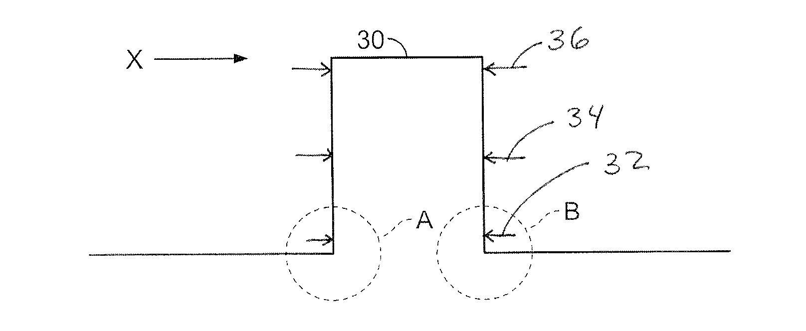
[0058]The preferred embodiments are directed to a method and corresponding apparatus for high speed imaging sample features, particularly those characterized by transition regions, such as that encountered when imaging a flat-to-sidewall region of a feature of a semiconductor sample. By detecting the flat-to-sidewall transition, and confirming the same, the sample in that region is then re-scanned to accurately measure the transition, including the entire base of the region. The method may operate in conjunction with a control method associated with operating an atomic force microscope in the above-described CD mode or a similar mode. Notably, the method operates independent of the specific dynamics of the scanner by re-scanning regions of the sample that typically would cause missing or biased data, i.e., notching, when imaging the sample using standard CD mode.

[0059]Turning initially to FIGS. 5A-5D, high speed operation of an AFM according to a preferred embodiment of the present ...


PUM


Abstract

A method and apparatus of scanning a sample with a scanning probe microscope including scanning a surface of the sample according to at least one scan parameter to obtain data corresponding to the surface, and substantially automatically identifying a transition in the surface. Based on the identified transition, the sample is re-scanned. Preferably, the resultant data is amended with data obtained by re-scanning the transition.

Description

BACKGROUND OF THE INVENTION[0001]1. Field of the Invention[0002]The present invention is directed to a method and apparatus for scanning a sample using a scanning probe microscope, and more particularly, to a method and apparatus of detecting a transition region in a sample and re-scanning the transition region.[0003]2. Description of Related Art[0004]Several probe-based instruments monitor the interaction between a cantilever-based probe and a sample to obtain information concerning one or more characteristics of the sample. As throughput requirements increase, increased data acquisition speeds are desired, thus making the ability to obtain reliable data a challenge.[0005]Scanning probe microscopes (SPMs), such as the atomic force microscope (AFM), are devices which typically use a sharp tip to make a local measurement of one or more properties of a sample. More particularly, SPMs typically characterize the surfaces of such small-scale sample features by monitoring the interaction ...

Claims


Application Information

Patent Timeline
IPC IPC(8): G01B5/28G01Q10/06G01Q30/06G01Q60/38
CPCB82Y35/00G01Q60/38G01Q30/06G01Q10/06H01L22/00
Inventor MININNI, PAUL L.
Owner BRUKER NANO INC
Why Eureka
Try Eureka