Driving voltage output circuit
- Summary
- Abstract
- Description
- Claims
- Application Information
AI Technical Summary
Benefits of technology
Problems solved by technology
Method used
Image
Examples
embodiment 1
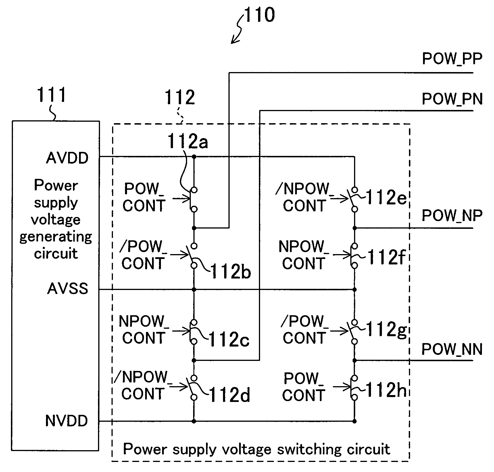
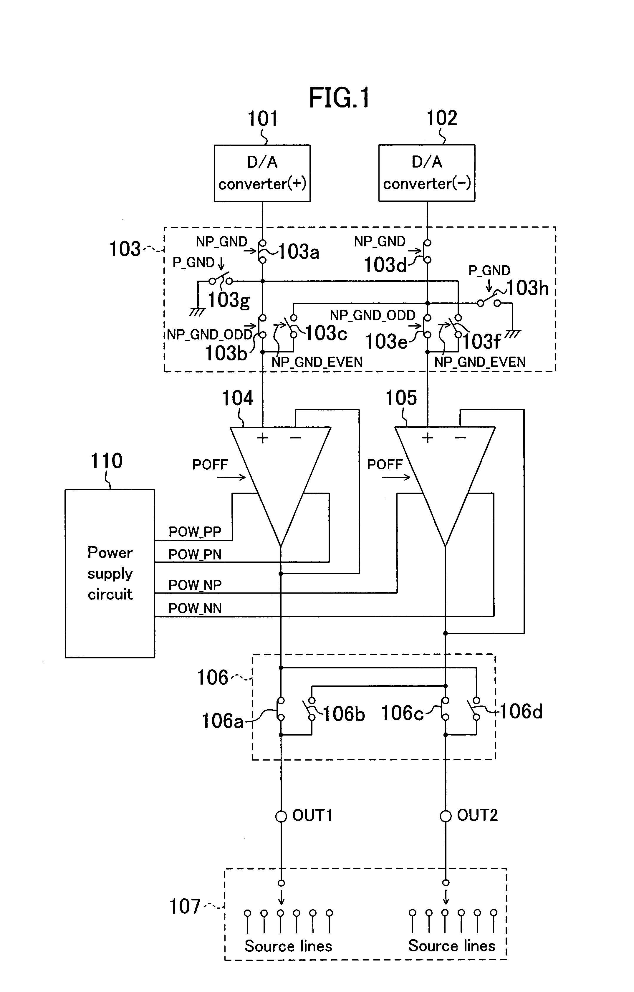
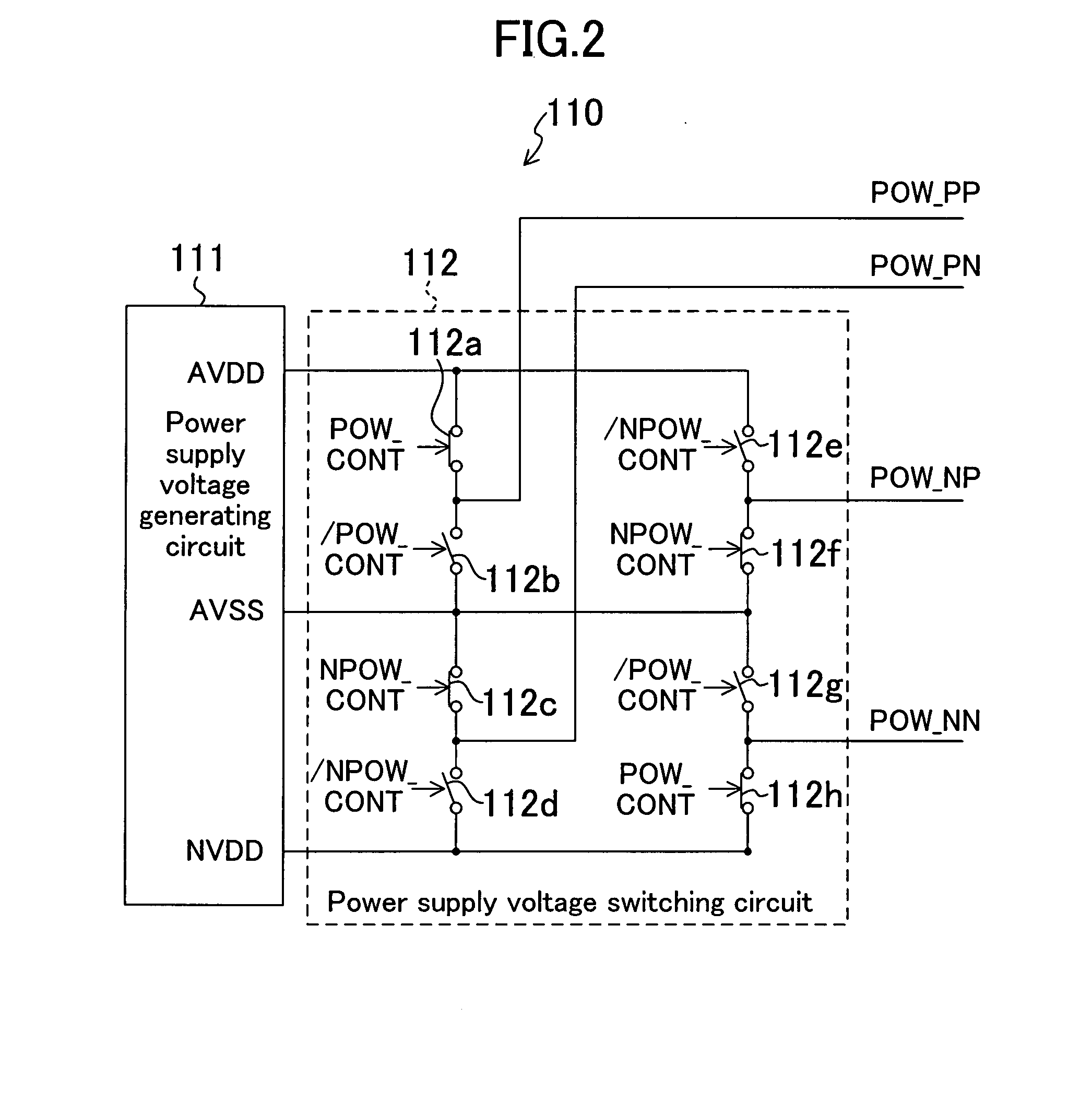
[0021]FIG. 1 is a circuit diagram showing a structure of a driving voltage output circuit for applying driving voltages to a predetermined number of source lines of, for example, a liquid crystal panel. The driving voltage output circuit includes: D / A converters 101, 102 for respectively outputting positive and negative image singal voltages on the basis of image data of the pixels; an input selector 103 for selectively exchanging the outputs of the D / A converter 101, 102; amplifiers 104, 105 of which each gain is, for example, one time; an output selector 106 for selectively exchanging the outputs of the amplifiers 104, 105; a distributing circuit 107 for connecting the output of the output selector 106 sequentially to the source lines; and a power supply circuit 110 for supplying two power supply voltages to each amplifier 104, 105.
[0022]The input selector 103 includes switches 103a to 103f for exchanging the sites where the image signal voltages from the respective D / A converters...
embodiment 2
[0064]Various kinds of amplifiers operated by two power supply voltages, such as operational amplifiers can be employed as the amplifiers 104, 105. While, the amplifiers 104, 105 are only require to output positive and negative driving voltages selectively, as described above, and accordingly can be simplified and reduced in its circuit scale when the states of the amplifiers can be selectively exchanged between a current source state and a current sink state.
[0065]Specifically, the amplifier 104 is composed of, as shown in FIG. 5, a differential section 201, an active load section 202, and an output section 203, similarly to general operational amplifiers. The output section 203 includes a P-channel transistor 203a, switches 203b, 203c, constant current sources 203d, 203e, switches 203f, 203g, and an N-channel transistor 203h. An output section 204 of the amplifier 105 has the same configuration as the output section 203 of the amplifier 104. In the output section 203 of the amplif...
embodiment 3
[0068]The amplifiers 104, 105 may have configurations shown in FIG. 7. In the example shown in FIG. 7, each output section 205, 206 includes transistors 205i, 205j in place of the switches 203b, 203g of the above-described output sections 203, 204. The transistors 205i, 205j control the gate potential of the transistors 203a, 203h, respectively, to turn the respective transistors 203a, 203h ON / OFF forcedly. With this configuration, though the switching speed is liable to decrease when compared with that in Embodiment 2, influence of ON resistance of the switches 203b, 203g can be avoided.
PUM
 Abstract
Description
Claims
Application Information


