

Method of Manufacturing Non-Volatile Memory Device
- Summary
- Abstract
- Description
- Claims
- Application Information
AI Technical Summary
Benefits of technology
Problems solved by technology
Method used
Image

Examples
Embodiment Construction
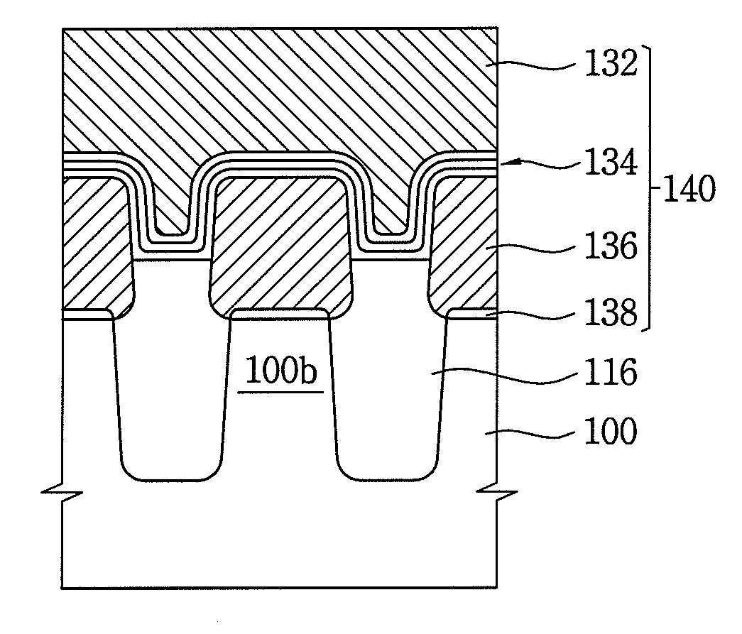
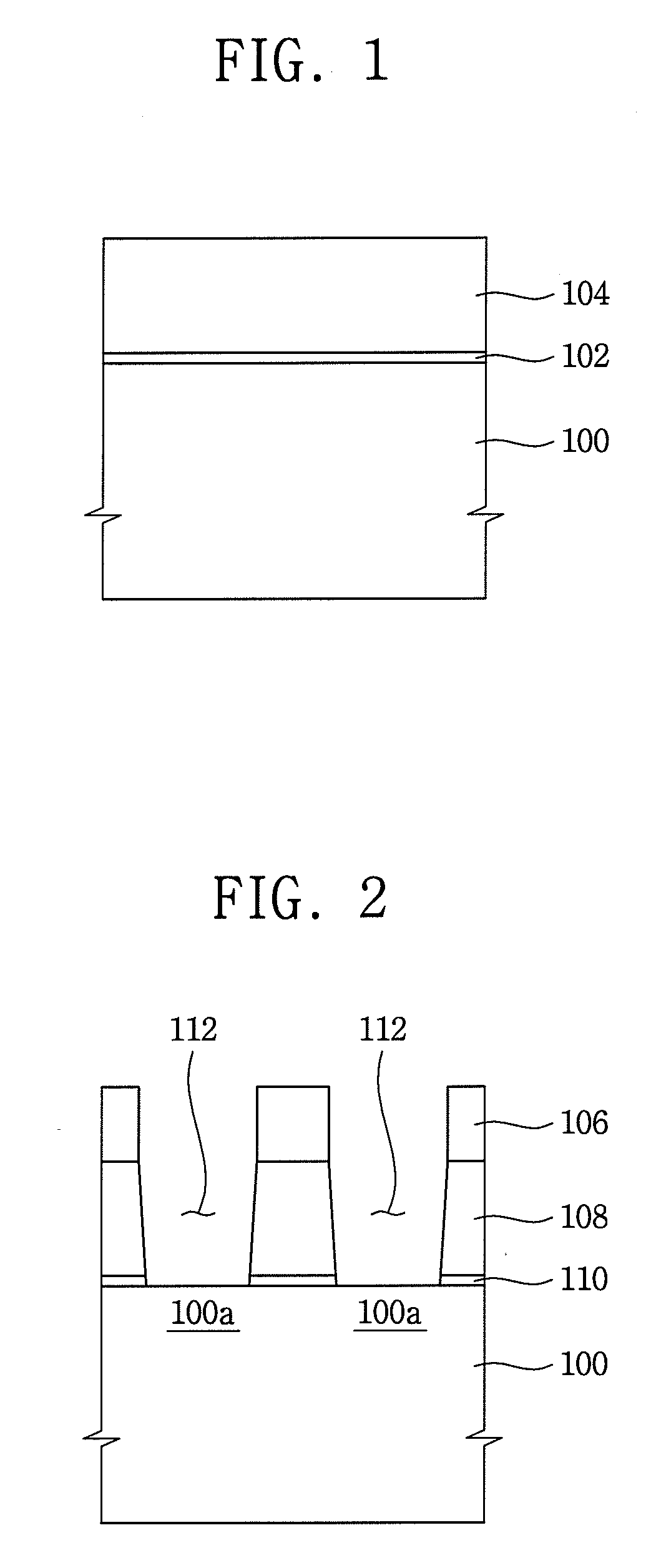
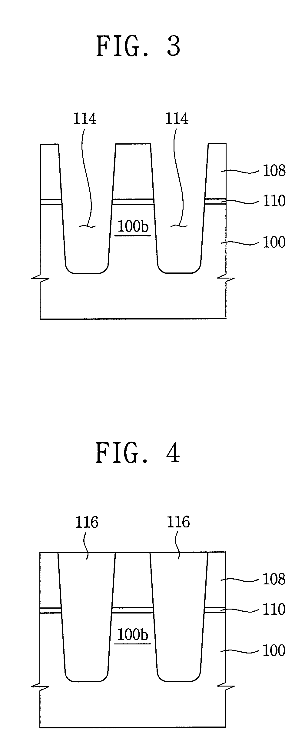
[0025]The present invention may, however, be embodied in many different forms and should not be construed as limited to the exemplary embodiments set forth herein. Like reference numerals refer to like elements throughout.
[0026]It will be understood that when an element is referred to as being “on” another element, it can be directly on the other element or intervening elements may be present. In contrast when an element is referred to as being “directly on” another element, there are no intervening elements present. As used herein, the term “and / or” includes any and all combinations of one or more of the associated listed items.
[0027]It will be understood that, although the terms first, second, etc. may be used herein to describe various elements, these elements should not be limited by these terms. These terms are only used to distinguish one element from another. For example, a first thin film could be termed a second thin film, and, similarly, a second thin film could be termed ...
PUM
 Abstract
Description
Claims
Application Information