
Method of manufacturing semiconductor device

a manufacturing method and semiconductor technology, applied in semiconductor devices, semiconductor/solid-state device details, electrical equipment, etc., can solve the problems of increased cost, increased process steps, inability to manufacture, etc., and achieve low-cost manufacturing, stable electrical connection, and stable writing characteristic

Active Publication Date: 2008-04-17
MICRON TECH INC
View PDF8 Cites 7 Cited by
  • Summary
  • Abstract
  • Description
  • Claims
  • Application Information

AI Technical Summary

Benefits of technology

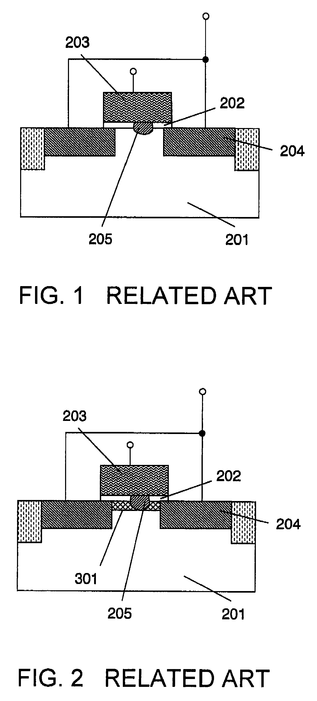
[0013]As described above, there is currently a problem that electrical connection at a breakdown location becomes instable during writing to an antifuse element. When an N− diffusion layer is formed to solve this problem, there occurs other problems such as increased number of process steps and increased cost. In view of these problems, it is an object of the present invention to provide a method of manufacturing an antifuse element without involving increase in cost.
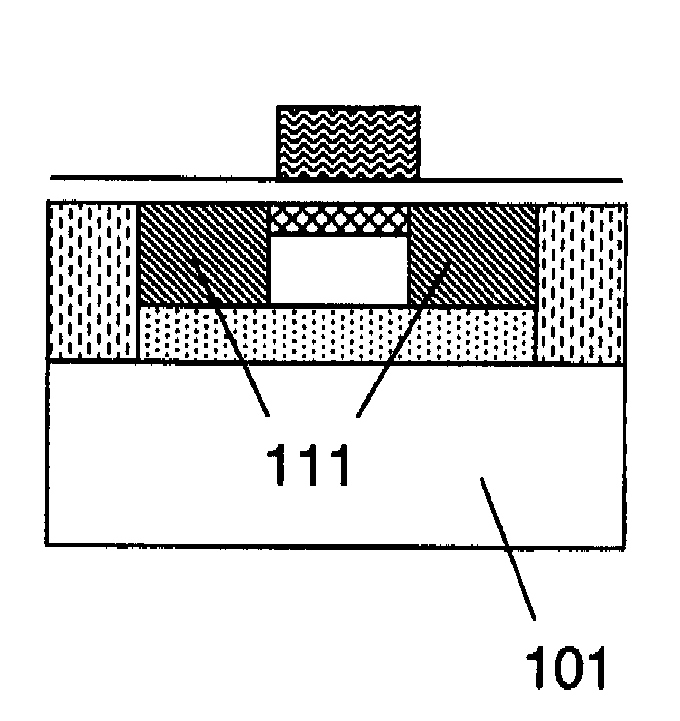
[0023]The method of manufacturing a semiconductor device according to the present invention forms an N− diffusion layer to be a source / drain diffusion region of the grooved transistor simultaneously with an N− diffusion layer of a channel region directly below the gate of the antifuse element. The formation of the N− diffusion layer directly below the gate of the antifuse element ensures stable electrical connection between the gate electrode and the source / drain diffusion region even if the breakdown of the antifuse element caused by writing is small. Therefore, an advantageous effect can be obtained that the writing to the antifuse element is possible at a relatively low voltage. Further, the simultaneous formation of the N− diffusion layers eliminates the need of increasing the number of process steps or the cost especially for formation of the antifuse element, and thus enables low-cost manufacture. According to the method of manufacturing a semiconductor device of the present invention, an antifuse element having a stable writing characteristic and a semiconductor device having such an antifuse element can be obtained without involving increase in the number of process steps or cost.

Problems solved by technology

As described above, there is currently a problem that electrical connection at a breakdown location becomes instable during writing to an antifuse element.
When an N− diffusion layer is formed to solve this problem, there occurs other problems such as increased number of process steps and increased cost.

Method used


Image

  • Method of manufacturing semiconductor device
  • Method of manufacturing semiconductor device
  • Method of manufacturing semiconductor device

Examples


Embodiment Construction

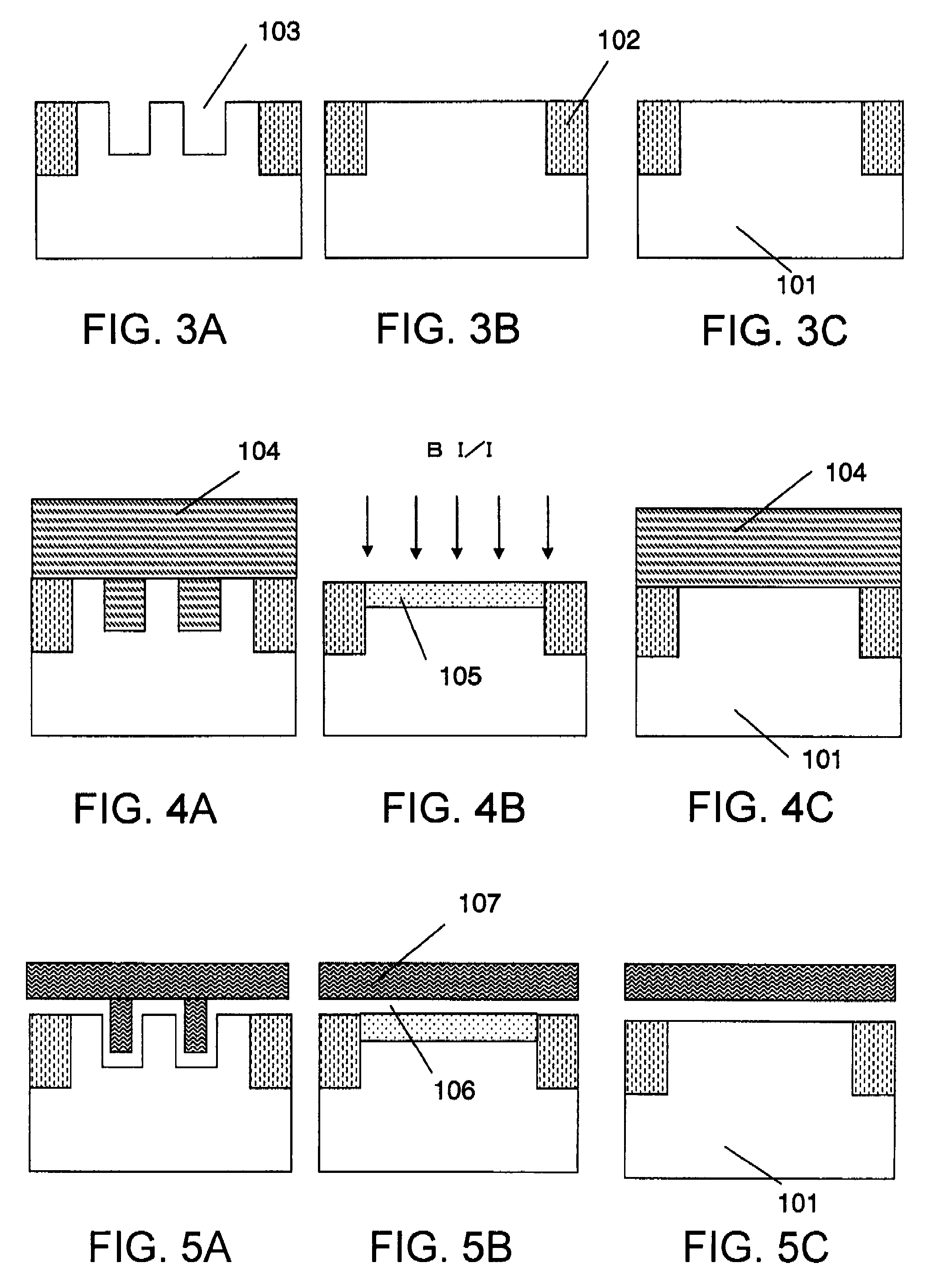
[0031]A method of manufacturing a semiconductor device according to the present invention will be described with reference to FIGS. 3 to 7. FIGS. 3 to 7 are cross-sectional views showing principal steps of the method of manufacturing a semiconductor device. The left side diagram with the alphabetic suffix “A” of each figure is a cross-sectional view showing a grooved memory cell portion formed by a grooved NMOS transistor, the central diagram with the alphabetic suffix “B” is a cross-sectional view showing an ordinary NMOS transistor portion, and the right side diagram with alphabetic suffix “C” is a cross-sectional view showing an antifuse element portion. Description herein will be made principally of formation of a transistor relating to the nature of the present invention.

[0032]At first, an element isolation trench with a depth of 250 nm for example is formed in the surface of a P-type semiconductor substrate 101 by a commonly used method. The trench is then filled with an eleme...


PUM


Abstract

A method of manufacturing a semiconductor device forms an N− diffusion layer to be a source / drain region of a grooved transistor simultaneously with an N− diffusion layer of a channel region directly under a gate electrode of an antifuse element. The formation of the N− diffusion layer directly under the gate electrode of the antifuse element stabilizes electrical connection between the gate electrode and the source / drain diffusion region even during writing with a low write voltage.

Description

[0001]This application is based upon and claims the benefit of priority from Japanese patent application No. 2006-279521, filed on Oct. 13, 2006, the disclosure of which is incorporated herein in its entirety by reference.BACKGROUND OF THE INVENTION[0002]1. Field of the Invention[0003]The present invention relates to a method of manufacturing a semiconductor device, and in particular to a method of manufacturing a semiconductor device having a grooved transistor and an antifuse element.[0004]2. Description of the Related Art[0005]The semiconductor device technology has been evolved year by year, enlarging the scale and capacity of semiconductor devices. As for typical semiconductor storage devices, for example, 1 Gbit dynamic random access memories (DRAMs) have been commercialized. Such large-capacity semiconductor devices employ a redundant circuit for substituting and remedying a defective memory cell. The redundant circuit remedies a defective memory cell by storing an address of...

Claims


Application Information

Patent Timeline
Patent Type & Authority Applications(United States)
IPC IPC(8): H01L21/336
CPCH01L23/5252H01L27/11206H01L27/112H01L2924/0002H10B20/00H10B20/25H01L2924/00H10B20/20
Inventor MANABE, KAZUTAKAKITAMURA, EIJI
Owner MICRON TECH INC
Learn More