Methods of etching polysilicon and methods of forming pluralities of capacitors

a polysilicon and polysilicon technology, applied in the field of etching polysilicon and to the method of forming pluralities of capacitors, can solve the problems of difficult to etch extremely deep capacitor electrode openings within doped silicon dioxide, capacitor electrodes,

Active Publication Date: 2008-04-17
MICRON TECH INC
View PDF98 Cites 76 Cited by
  • Summary
  • Abstract
  • Description
  • Claims
  • Application Information

AI Technical Summary

Problems solved by technology

As integrated circuitry density has increased, there is a continuing challenge to maintain sufficiently high storage capacitance despite typical decreasing capacitor area.
Such dimensional variations result in the capacitor electrode openings needing to be etched deeper into the capacitor electrode-forming material.
It is difficult to etch extremely deep capacitor electrode openings within doped silicon dioxides, such as phosphosilicate glass (PSG).

Method used


Image

  • Methods of etching polysilicon and methods of forming pluralities of capacitors
  • Methods of etching polysilicon and methods of forming pluralities of capacitors
  • Methods of etching polysilicon and methods of forming pluralities of capacitors

Examples


Embodiment Construction

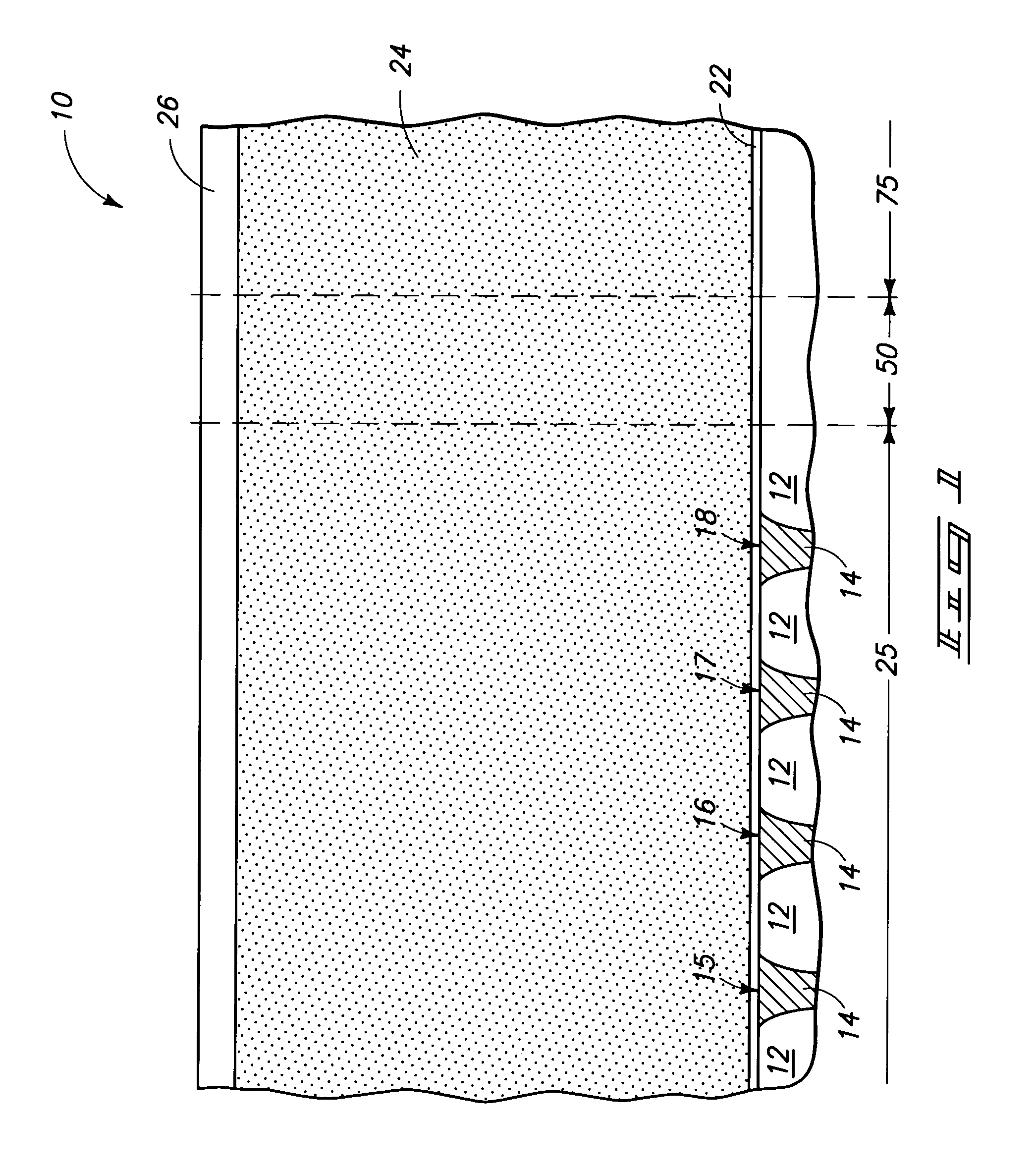
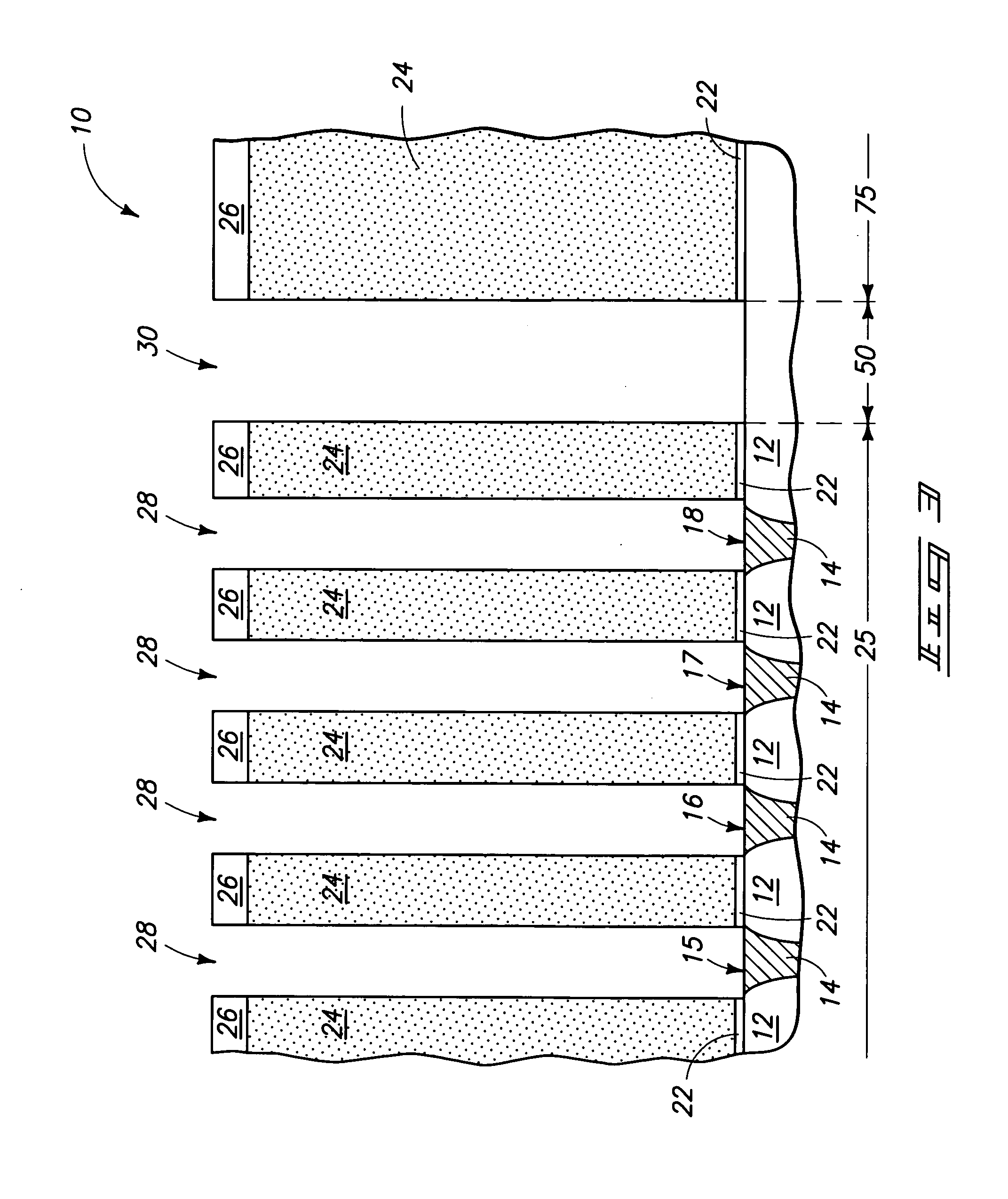
[0020]Embodiments are described below primarily in the context of fabricating a plurality of capacitors, for example in an array of capacitors in the fabrication of DRAM. However, the invention is in no way so limited, encompassing fabrication of other integrated circuitry and encompassing any method of etching polysilicon from any substrate.

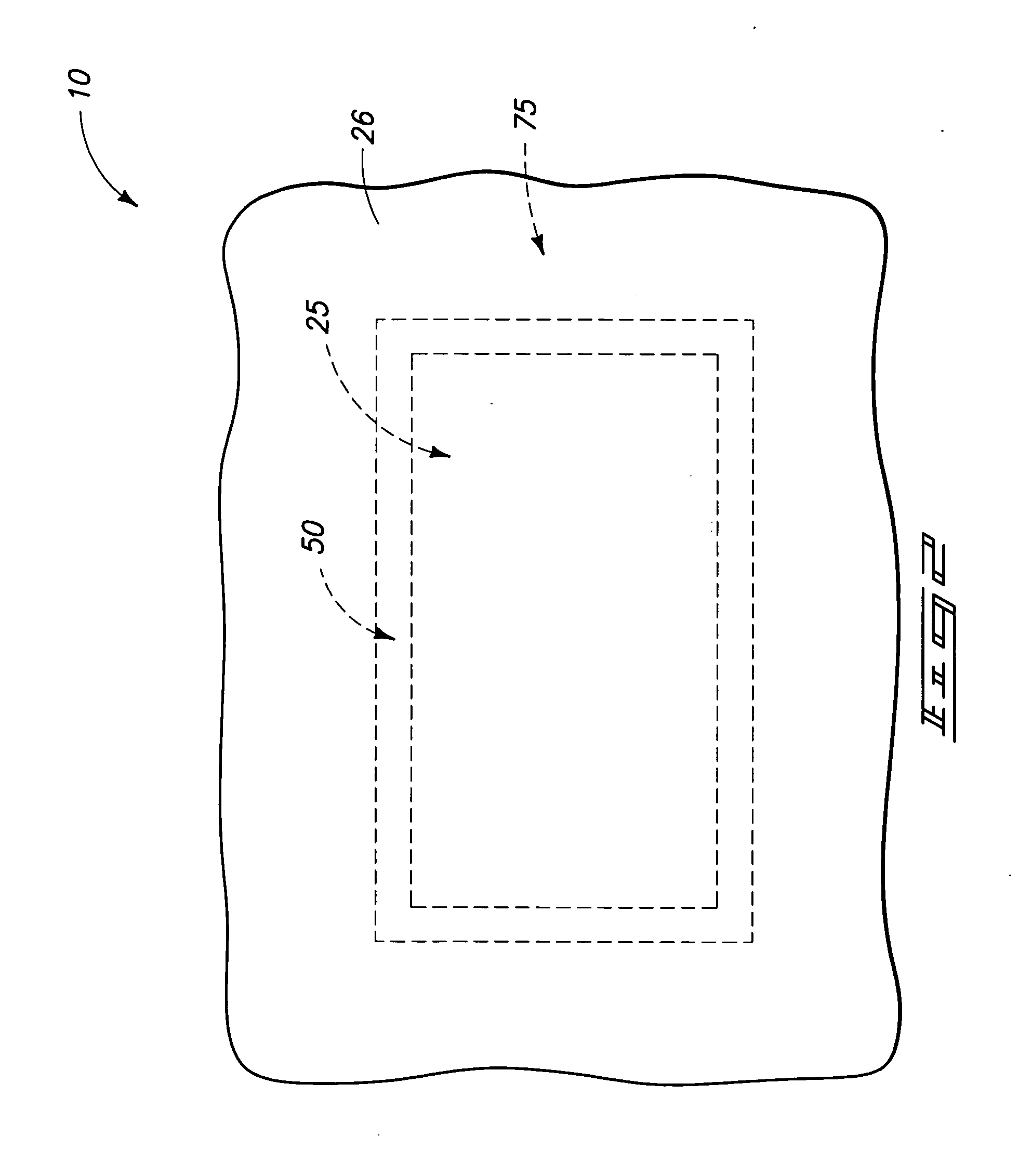
[0021]Embodiments of methods of forming pluralities of capacitors are described with reference to FIGS. 1-14. Referring initially to FIGS. 1 and 2, a substrate, such as a semiconductor substrate, is indicated generally with reference numeral 10. In the context of this document, the term “semiconductor substrate” or “semiconductive substrate” is defined to mean any construction comprising semiconductive material, including, but not limited to, bulk semiconductive materials such as a semiconductive wafer (either alone or in assemblies comprising other materials thereon), and semiconductive material layers (either alone or in assemblies comprising ...


PUM

PropertyMeasurementUnit
pressureaaaaaaaaaa
temperatureaaaaaaaaaa
thicknessaaaaaaaaaa

Abstract

A method of etching polysilicon includes exposing a substrate comprising polysilicon to a solution comprising water, HF, and at least one of a conductive metal nitride, Pt, and Au under conditions effective to etch polysilicon from the substrate. In one embodiment, a substrate first region comprising polysilicon and a substrate second region comprising at least one of a conductive metal nitride, Pt, and Au is exposed to a solution comprising water and HF. The solution is devoid of any detectable conductive metal nitride, Pt, and Au prior to the exposing. At least some of the at least one are etched into the solution upon the exposing. Then, polysilicon is etched from the first region at a faster rate than any etch rate of the first region polysilicon prior to the etching of the at least some of the conductive metal nitride, Pt, and Au.

Description

TECHNICAL FIELD[0001]Embodiments disclosed herein pertain to methods of etching polysilicon and to methods of forming pluralities of capacitors.BACKGROUND OF THE INVENTION[0002]Capacitors are one type of component commonly used in the fabrication of integrated circuits, for example in DRAM and other circuitry. A typical capacitor is comprised of two conductive electrodes separated by a non-conducting dielectric region. As integrated circuitry density has increased, there is a continuing challenge to maintain sufficiently high storage capacitance despite typical decreasing capacitor area. The increase in density of integrated circuitry has typically resulted in greater reduction in the horizontal dimension of capacitors as compared to the vertical dimension. In many instances, the vertical dimension of capacitors has increased.[0003]Several techniques have been developed to increase the storage capacity of a capacitor. One such technique is to fabricate a capacitor wherein at least o...

Claims


Application Information

Patent Timeline
Patent Type & Authority Applications(United States)
IPC IPC(8): H01L21/302
CPCH01L21/32134
Inventor RAGHU, PRASHANTBHAT, VISHWANATHRANA, NIRAJ
Owner MICRON TECH INC
Why Eureka
Try Eureka