LED package and manufacturing method thereof

a technology of led packaging and manufacturing method, which is applied in the direction of semiconductor/solid-state device manufacturing, semiconductor devices, electrical devices, etc., can solve the problems of lowering the strength of the adhering layer b>150/b> or even damaging the adhering layer, low productivity, waste of process time, etc., and achieves the effect of reducing production cost and increasing heat dissipation efficiency

Inactive Publication Date: 2008-04-24
YOUNG LIGHTING TECHNOLOGY INC
View PDF9 Cites 12 Cited by
  • Summary
  • Abstract
  • Description
  • Claims
  • Application Information

AI Technical Summary

Benefits of technology

[0008]The present invention is directed to a light emitting diode (LED) packa

Problems solved by technology

Furthermore, the thermal stress produced by the heat will easily lead to a lowering of the strength of the adhering layer 150 or even damage the adhering layer 150.
However, the curing process wastes a lot of time and leads to low productivity.
Moreover, the adhesive strength of the silver epoxy may vary according to t

Method used


Image

  • LED package and manufacturing method thereof
  • LED package and manufacturing method thereof
  • LED package and manufacturing method thereof

Examples


Embodiment Construction

[0019]It is to be understood that other embodiments may be utilized and structural changes may be made without departing from the scope of the present invention. Also, it is to be understood that the phraseology and terminology used herein is for the purpose of description and should not be regarded as limiting. The use of “including,”“comprising,” or “having” and variations thereof herein is meant to encompass the items listed thereafter and equivalents thereof as well as additional items. Unless limited otherwise, the terms “connected,” and “coupled,” and variations thereof herein are used broadly and encompass direct and indirect connections, couplings, and mountings.

[0020]Reference will now be made in detail to the present preferred embodiments of the invention, examples of which are illustrated in the accompanying drawings. Wherever possible, the same reference numbers are used in the drawings and the description to refer to the same or like parts.

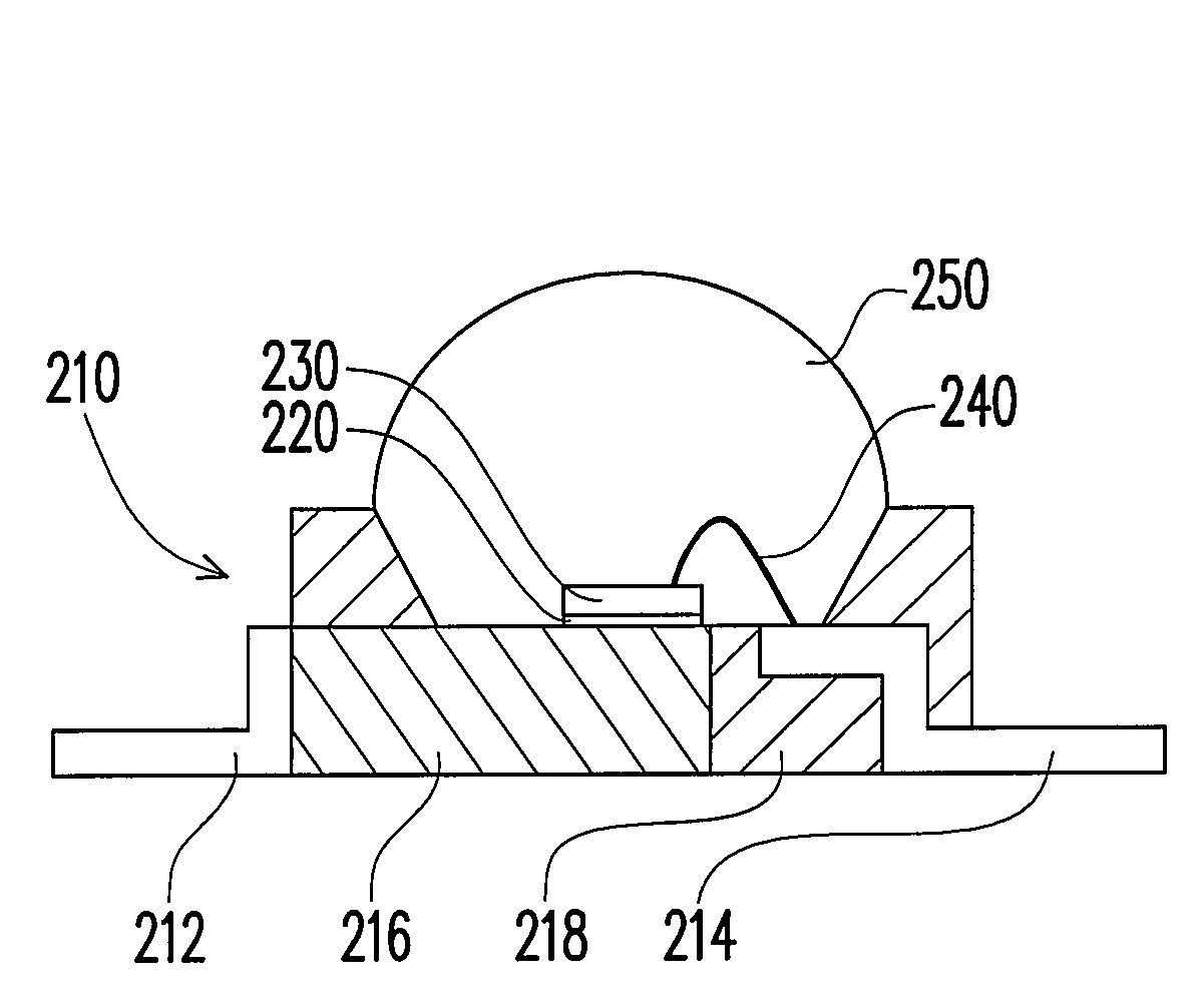
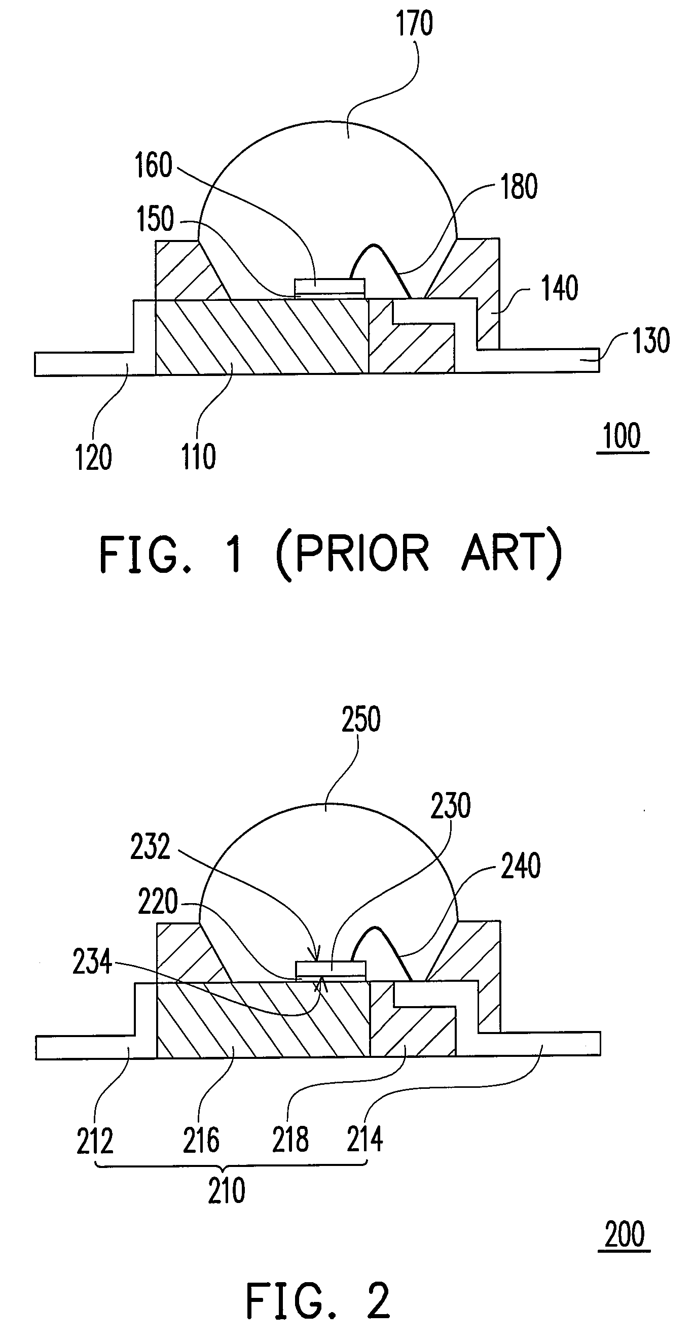
[0021]FIG. 2 is a schematic di...


PUM


Abstract

A light emitting diode (LED) package including a carrier, an adhering layer and an LED chip is provided. The adhering layer is disposed on the carrier. The LED chip is disposed on the adhering layer and electrically connected to the carrier. The material of the adhering layer comprises a lead-free tin-based eutectic alloy. Furthermore, a manufacturing method for the LED package is provided.

Description

CROSS-REFERENCE TO RELATED APPLICATION[0001]This application claims the priority benefit of Taiwan application serial no. 95138336, filed Oct. 18, 2006. All disclosure of the Taiwan application is incorporated herein by reference.BACKGROUND OF THE INVENTION[0002]1. Field of the Invention[0003]The present invention relates to a light emitting device package, and more particularly to a light emitting diode (LED) package and manufacturing method thereof.[0004]2. Description of Related Art[0005]FIG. 1 is a schematic diagram of a conventional light emitting diode (LED) package. As shown in FIG. 1, the LED package 100 includes a heat slug 110, a first lead 120, a second lead 130, a housing 140, an adhering layer 150, an LED chip 160 and a molding compound 170. The heat slug 110 is disposed between the first lead 120 and the second lead 130 and is electrically connected to the first lead 120. The housing 140 is used for fixing the heat slug 110, the first lead 120 and the second lead 130. ...

Claims


Application Information

Patent Timeline
IPC IPC(8): H01L33/00H01L33/62H01L33/64
CPCH01L33/62H01L2224/83192H01L2224/48091H01L2224/48247H01L2224/73265H01L2924/01079H01L33/641H01L24/83H01L24/29H01L2224/92247H01L2224/32257H01L2224/32245H01L2924/01019H01L2924/01322H01L2924/01029H01L2924/00014H01L2924/00H01L2924/351H01L2924/181H01L2924/12041H01L2924/00012
Inventor LEE, LIANG-CHIHYANG, CHIAO-CHIHWANG, CHIEN-MIN
Owner YOUNG LIGHTING TECHNOLOGY INC
Why Eureka
Try Eureka