Semiconductor device and method of fabricating the same

a technology of semiconductor devices and semiconductors, applied in semiconductor devices, semiconductor/solid-state device details, electrical apparatus, etc., can solve problems such as increasing the difficulty of forming small contact holes using conventional techniques, reducing the size of a bit line used in memory devices, and presenting several problems. to achieve the effect of preventing electrical contact failur

Active Publication Date: 2008-04-24
SAMSUNG ELECTRONICS CO LTD
View PDF5 Cites 19 Cited by
  • Summary
  • Abstract
  • Description
  • Claims
  • Application Information

AI Technical Summary

Benefits of technology

[0009]Embodiments of the present invention provide a semiconductor device which can prevent electrical contact failures.
[0010]Embodiments of the present invention also provide a method of fabricating a semiconductor device which can prevent electrical contact failures.

Problems solved by technology

As a result, forming small contact holes using conventional techniques becomes increasingly difficult with further integration of semiconductor devices.
In this regard, several problems may be presented.
For example, the size of the contact hole gradually decreases at the region of contact with the lower interconnection line, or the formation of contact holes using a photolithography process in highly integrated semiconductor devices can lead to unreliable results.
Meanwhile, as the integration of semiconductor devices increases, the size of a bit line used in memory devices becomes further reduced, and a margin for insulating an underlying pad becomes insufficient during the wet etch process performed for the purpose of increasing the size of the buried contact, thereby increasing the likelihood of partial exposure of an adjacent pad.
Accordingly, an etching solution may penetrate through a direct contact (DC) that electrically connects the bit line to an underlying contact pad, so that a conductive material can become erroneously etched.
In particular, a silicide layer formed at an interface between the contact pad and the direct contact (DC) can become easily damaged by an etching solution.
Therefore, the direct contact (DC) of the underlying bit line may be partially filled with an insulating material or a conductive material of a buried contact (BC) in a subsequent process, thereby resulting in unwanted electrical contact failures in the manufacture of semiconductor devices.

Method used


Image

  • Semiconductor device and method of fabricating the same
  • Semiconductor device and method of fabricating the same
  • Semiconductor device and method of fabricating the same

Examples


Embodiment Construction

[0038]Advantages and features of the embodiments of the present invention and methods of accomplishing the same may be understood more readily by reference to the following detailed description of preferred embodiments and the accompanying drawings. The present invention may, however, be embodied in many different forms and should not be construed as being limited to the embodiments set forth herein. Rather, these embodiments are provided so that this disclosure will be thorough and complete, and the embodiments of the present invention will only be defined by the appended claims. Like reference numerals refer to like elements throughout the specification.

[0039]The present invention now will be described more fully hereinafter with reference to the accompanying drawings, in which preferred embodiments are shown.

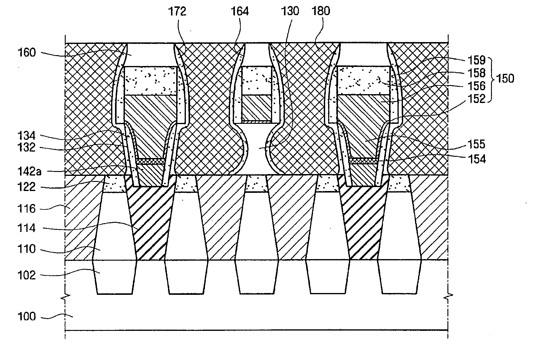
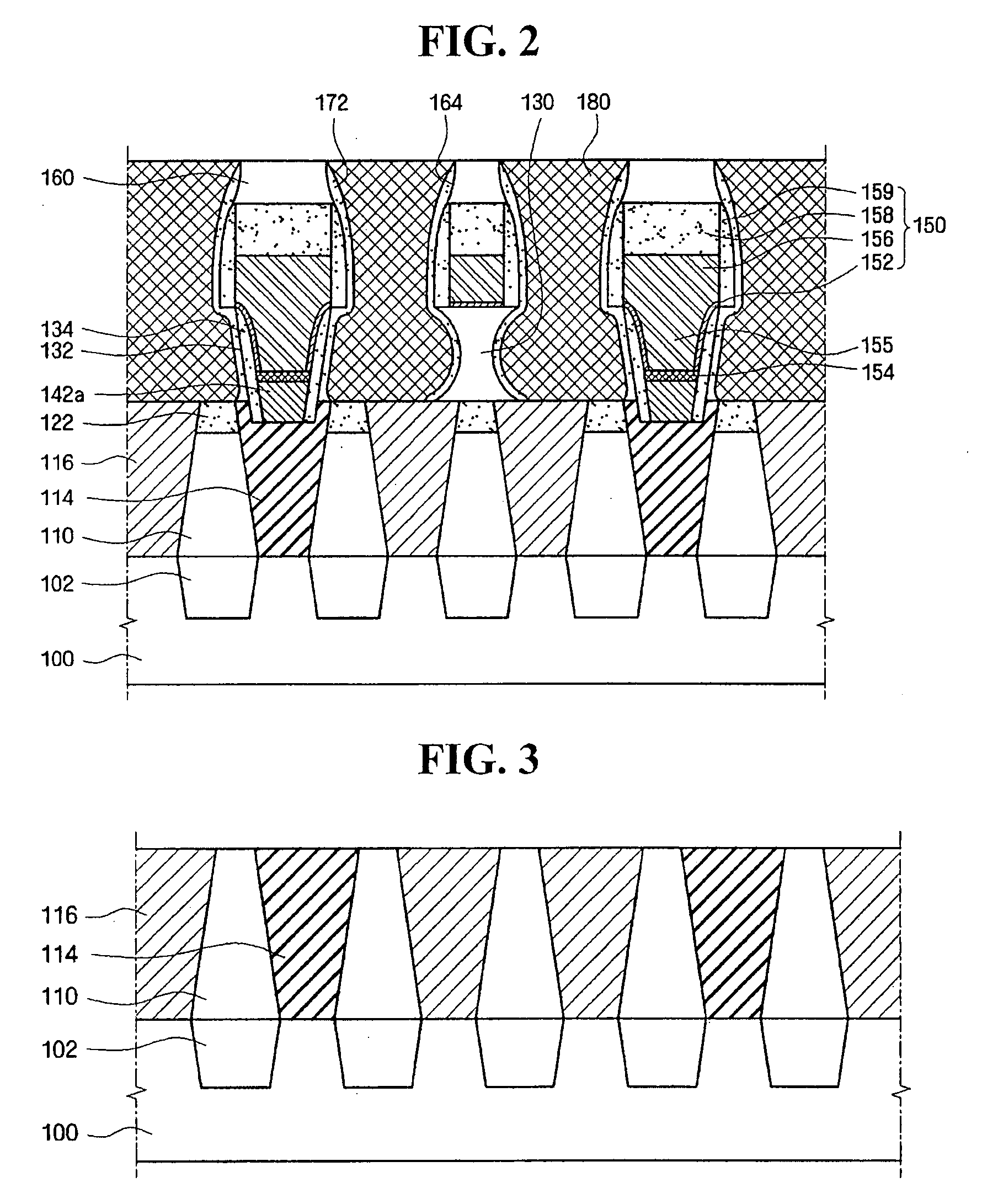
[0040]A structure of a semiconductor device according to an embodiment of the present invention will now be described with reference to FIGS. 1 and 2.

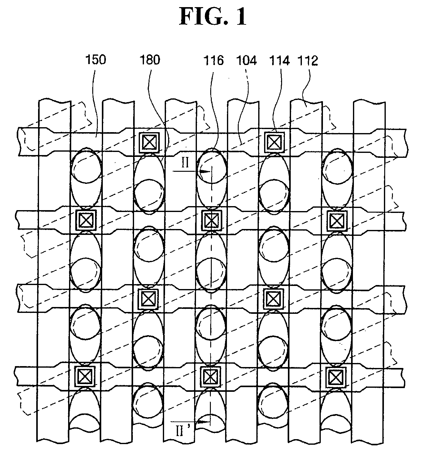
[0041]FIG. 1 is a layout...


PUM


Abstract

In a semiconductor device and a method of fabricating the same, the semiconductor device includes a contact pad in a first interlayer insulating layer on a semiconductor substrate, a contact hole in a second interlayer insulating layer on the first interlayer insulating layer, selectively exposing the contact pad, a contact spacer on internal walls of the contact hole, a first contact plug connected to the contact pad exposed by the contact hole having the contact spacer on the internal walls thereof, the first contact plug partially filling the contact hole, a metal silicide layer on a surface of the first contact plug, and a second contact plug on the metal silicide layer and partially filling the remaining portion of the contact hole.

Description

CROSS-REFERENCE TO RELATED APPLICATION[0001]This application claims priority from Korean Patent Application No. 10-2006-0102443 filed on Oct. 20, 2006 in the Korean Intellectual Property Office, the disclosure of which is incorporated herein by reference in its entirety.BACKGROUND OF THE INVENTION[0002]1. Field of the Invention[0003]The present invention relates to a semiconductor device and a method of fabricating the same, and more particularly, to a semiconductor device which can prevent electrical contact failures, and a method of fabricating the same.[0004]2. Description of the Related Art[0005]Higher integration in semiconductor devices has resulted in a decrease in the size of a contact hole that connects one element or layer to another element or layer, while resulting in an increase in the relative thickness of an interlayer insulating layer. Thus, the aspect ratio of the contact hole increases, and an alignment margin of the contact hole decreases, in a photolithography pr...

Claims


Application Information

Patent Timeline
Patent Type & Authority Applications(United States)
IPC IPC(8): H01L23/52H01L21/4763
CPCH01L27/10814H01L27/10888H01L27/10885H01L27/10855H10B12/315H10B12/485H10B12/0335H10B12/482H01L21/28H01L21/3205
Inventor LEE, JIN-WON
Owner SAMSUNG ELECTRONICS CO LTD
Why Eureka
Try Eureka