
Drive Circuit for Insulated Gate Device

Active Publication Date: 2008-04-24
FUJI ELECTRIC CO LTD
View PDF8 Cites 48 Cited by
  • Summary
  • Abstract
  • Description
  • Claims
  • Application Information

AI Technical Summary

Benefits of technology

[0009]The invention addresses the problems discussed above, and aims to provide a drive circuit for an insulated gate device which can reduce loss at the time of turn-on and reduce temperature dependency of noise.
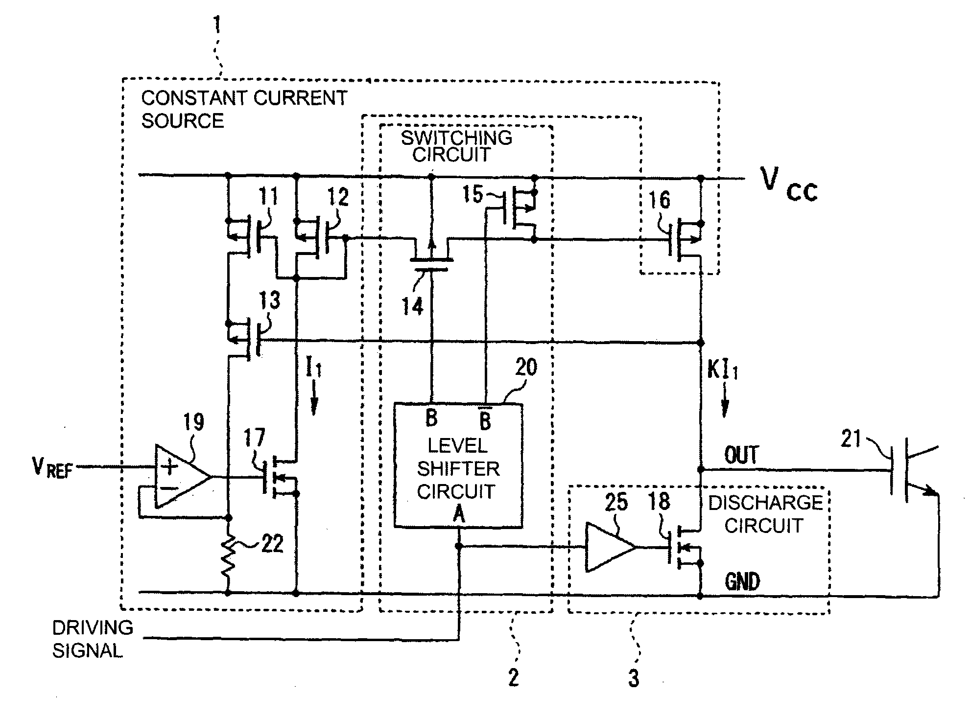
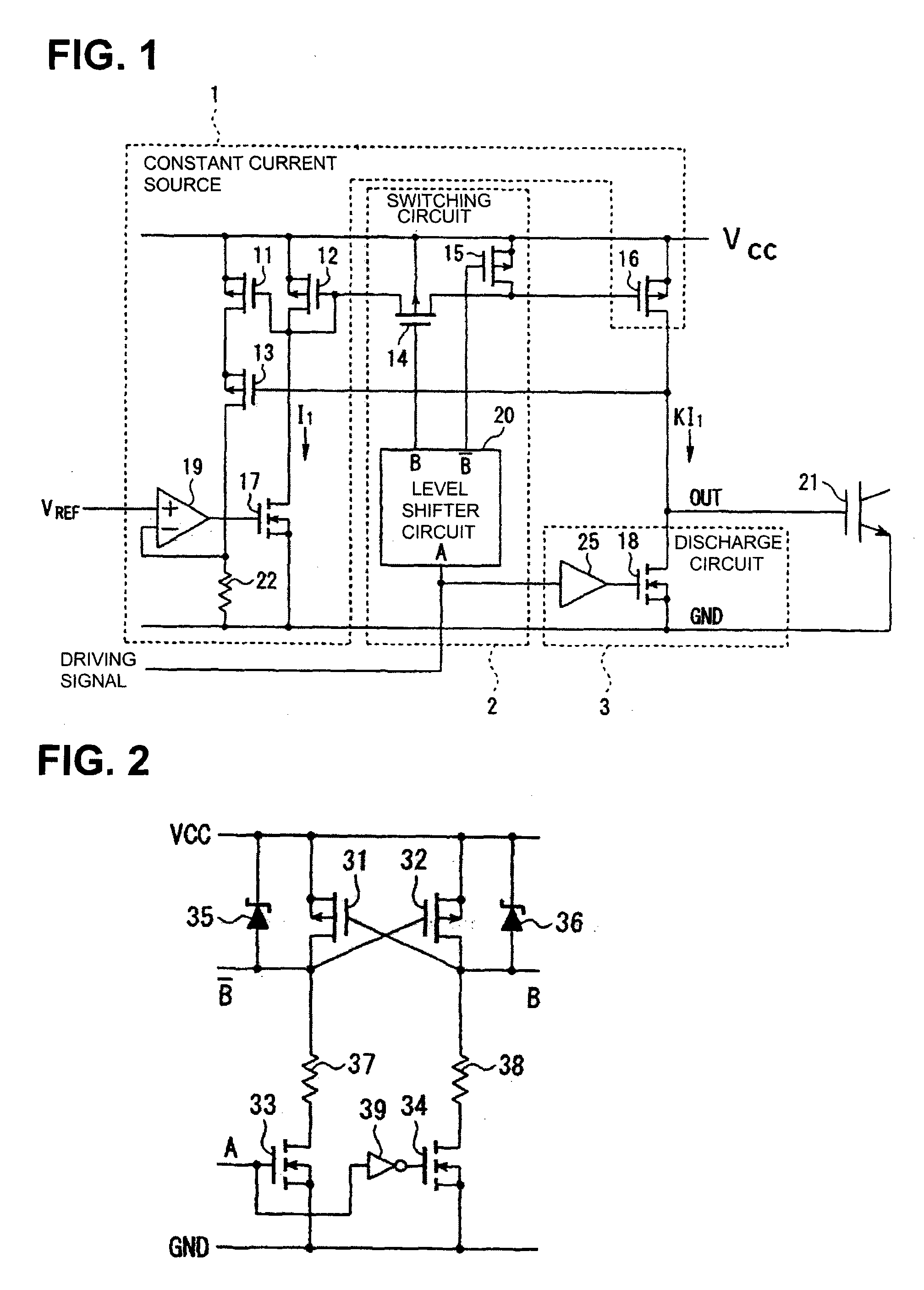
[0010]The invention provides a drive circuit for an insulated gate device which can reduce loss at the time of turn-on and reduce temperature dependency of noise, while solving the above problem. A drive circuit for an insulated gate device according to a first aspect of the invention is characterized by including a constant current source which generates a constant current, a switching circuit which a gate of the insulated gate device is connected to a power supply potential side via the constant current source at the time of turn-on and the gate of the insulated gate device is connected to a ground potential side at the time of turn-off, and a discharge circuit by which the insulated gate device is turned off. This makes it possible for the insulated gate device to turn on via the constant current source, and makes it possible to reduce temperature dependency of charging velocity of the gate of the insulated gate device. Because of this, while suppressing noise and loss at the time of turn-on in a high temperature condition, noise and loss can also be suppressed at room temperature.
[0011]The drive circuit for an insulated gate device according to a second aspect of the invention is characterized that, in the first aspect of the invention, the constant current source includes a first transistor of which a drain side is coupled to a resistor, a second transistor which is configured as a current mirror circuit along with the first transistor and which generates a constant current determined by the value of the resistor and a reference voltage and a third transistor which is configured as the current mirror circuit along with the second transistor and of which a drain is connected to the gate of the insulated gate device. By this, while amplifying the constant current determined by the value of the resistor and the reference voltage, the insulated gate device can be turned on, and while suppressing noise and loss at the time of turn-on in a high temperature condition, noise and loss can also be suppressed at a room temperature condition.

Problems solved by technology

In addition, when the insulated gate power device and the drive circuit are equipped in the same module, the drive circuit which is near the insulated gate power device is put under a severe thermal environment because the operating temperature of the insulated gate power device is guaranteed to a maximum of 150° C.
However, there is a problem in that loss increases so that a time needed for the turn-on of the IGBT 43 increases.
On the other hand, when the design is optimized for the high temperature condition in order to cause as little lose as possible, the charging velocity of the gate of the IGBT 43 is too fast at room temperature, and the voltage variation becomes steep, so that there is a problem that noise increases.

Method used


Image

  • Drive Circuit for Insulated Gate Device
  • Drive Circuit for Insulated Gate Device
  • Drive Circuit for Insulated Gate Device

Examples


first embodiment

[0024]Preferred embodiments of a drive circuit for an insulated gate device according to the invention will be now explained with reference to the accompanying drawings. FIG. 1 is a view showing the circuit configuration of a drive circuit for the insulated gate device according to the invention. While, by the following discussion, the IGBT is explained for example as the insulated gate device, a power MOSFET and the like other than the IGBT may be used as the insulated gate device. In FIG. 1, the drive circuit for an IGBT 21 includes a constant current source 1 generating a constant current, a switching circuit 2 which a gate of the IGBT 21 is connected to a power supply potential Vcc side at the time of turn-on and also the gate of the IGBT 21 is connected to a ground potential GND side at the time of turn-off and a discharge circuit 3 by which the IGBT 21 is turned off.

[0025]Here, the constant current source 1 includes a P-FET 11, a P-FET 12 and a P-FET 16 which are connected as ...

second embodiment

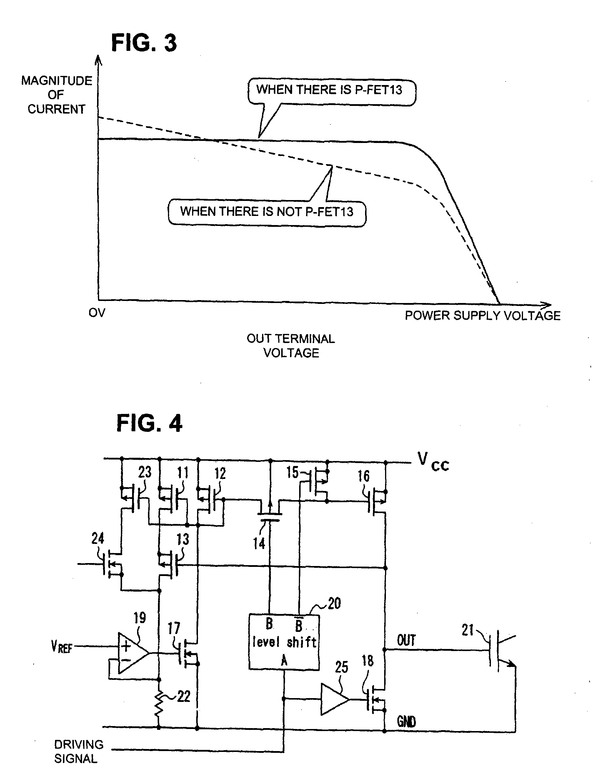
[0040]FIG. 4 is a view showing the circuit configuration of a drive circuit for the insulated gate device according to the invention. In FIG. 4, a P-FET 23 and an N-FET 24 are included in addition to the drive circuit for the IGBT 21 of FIG. 1. Here, a source of the P-FET 23 is connected to the power supply potential Vcc, and a drain of the P-FET 23 is connected to a drain of the N-FET 24. A gate of the P-FET 23 is connected to the gate of the P-FET 11. In addition, a source of the N-FET 24 is connected to the drain of the P-FET 13.

[0041]Here, when the gate potential of the IGBT 21 (OUT terminal voltage of the drive circuit) approaches the power supply potential Vcc, the gate potential of the N-FET 24 can be controlled so that the N-FET 24 turns on. For example, when the gate potential of the IGBT 21 has become (Vcc-2) volts, the N-FET 24 can be controlled so that the N-FET 24 turns on.

[0042]Current flows through the resistor 22 to the P-FET 23 configured as the current mirror circu...


PUM


Abstract

A drive circuit for an insulated gate device includes a constant current source generating a constant current, and a switching circuit, wherein a gate of the insulated gate device is connected to a power supply potential side via the constant current source at the time of turn-on and to a ground potential side at the time of turn-off. Whereby a drive circuit for the insulated gate device can be reduced loss at the time of turn-on and reduced temperature dependency of noise.

Description

CROSS-REFERENCE TO RELATED APPLICATION[0001]This application claims priority from Japanese Patent Application 2006-283740 filed on Oct. 18, 2006, the contents of which are incorporated herein by reference.BACKGROUND OF THE INVENTION[0002]The present invention relates to a drive circuit for an insulated gate device, and in particular to a drive circuit which is suitable for applying to a method for reducing loss of a drive circuit for an insulated gate device, and for reducing temperature dependency of noise due to an insulated gate device.[0003]In a semiconductor power converter, insulated gate power devices such as an insulated gate bipolar transistor (IGBT), a power MOSFET and the like are used, and there is a method in which a drive circuit for driving these insulated gate power devices is made using an inverter configuration. FIG. 5 is a view showing the circuit configuration of a drive circuit of a conventional insulated gate device.[0004]In FIG. 5, a P channel field effect tra...

Claims


Application Information

Patent Timeline
IPC IPC(8): H03K3/00
CPCH03K17/168H03K2217/0036H03K2017/0806H03K17/567
Inventor NAKAMORI, AKIRAOYABE, KAZUNORI
Owner FUJI ELECTRIC CO LTD
Learn More